

NTE NTE724 Datasheet
NTE724
Integrated Circuit
Differential/Cascode Amplifier
Description:
The NTE724 is a differential/cascode amplifier in an 8–Lead TO5 type metal can package designed
for use in communications and industrial equipment operating at frequencies from dc to 120MHz.
Features:
D Controlled for Input Offset Voltage, Input Offset Current, and Input Bias Current
D Balanced Differential Amplifier Configuration with Controlled Constant–Current Source
D Single and Dual–Ended Operation
Applications:
D RF and IF Amplifiers (Differential or Cascode)
D DC, Audio, and Sense Amplifiers
D Converter in the Commercial FM Band
D Oscillator
D Mixer
D Limiter
Absolute Maximum Ratings:
Power Dissipation (T
≤ +85°C), P
A
(TA = +25°C unless otherwise specified)
D
450mW. . . . . . . . . . . . . . . . . . . . . . . . . . . . . . . . . . . . . . . . . . . . . .
Derate Linearly Above 85°C 5mW/°C. . . . . . . . . . . . . . . . . . . . . . . . . . . . . . . . . . . . . . . . . . . . . . .
Operating Ambient Temperature Range, T
Storage Temperature Range, T
stg
Lead Temperature (During Soldering, 1/16” from case, 10sec max), T
Electrical Characteristics:
Parameter Symbol Test Conditions Min Typ Max Unit
Input Bias Current I
Quiescent Operating Current I6 or I8VCC = +6V, VEE = –6V 0.8 1.25 2.0 mA
AGC Bias Current (Into Constant
Current Source Pin7)
(TA = +25°C, VCC = +12V, VEE = –12V unless otherwise specified)
II
I
7
opr
L
VCC = +6V, VEE = –6V – 16.6 70.0 µA
VCC = 12V, V
VCC = 12V, V
= 9V – 1.28 – mA
AGC
= 12V – 1.65 – mA
AGC
–55° to +125°C. . . . . . . . . . . . . . . . . . . . . . . . . . . . . . . . .
–65° to +150°C. . . . . . . . . . . . . . . . . . . . . . . . . . . . . . . . . . . . . . . . . .
+265°C. . . . . . . . . . . . . . . . .
– 36 106 µA
2.0 3.3 5.0 mA
Electrical Characteristics (Cont’d): (TA = +25°C, VCC = +12V, VEE = –12V unless otherwise
specified)
Parameter Symbol Test Conditions Min Typ Max Unit
Input Current (Pin7) I
Device Dissipation P
Power Gain G
Noise Figure NF
Power Output (Untuned) P
AGC Range AGC
Voltage Gain A
Peak–to–Peak Output Current I
7
T
P
O
P–P
VCC = +6V, VEE = –6V 0.5 0.85 1.0 mA
1.0 1.65 2.1 mA
VCC = +6V, VEE = –6V 24 36 54 mW
120 175 260 mW
VCC = 9V,
f = 100MHz
VCC = 9V,
f = 10.7MHz
VCC = 9V,
f = 100MHz
VCC = 9V,
f = 10.7MHz
VCC = 0V,
f = 10.7MHz
R
= 1kΩ
L
VCC = 9V
VCC = 12V
Cascode 16 20 – dB
Differential Amp 14 17 – dB
Cascode 35 39 – dB
Differential Amp 28 32 – dB
Cascode – 7.2 9.0 dB
Differential Amp – 6.7 9.0 dB
Diff. Amp 50Ω Input–Output – 5.7 – µW
Differential Amp – 62 – dB
Cascode – 40 – dB
Differential Amp – 30 – dB
Differential Amp, f = 10.7MHz,
ein = 400mV
2.0 4.0 7.0 mA
3.5 6.0 10.0 mA
Output High
AGC
Output Low
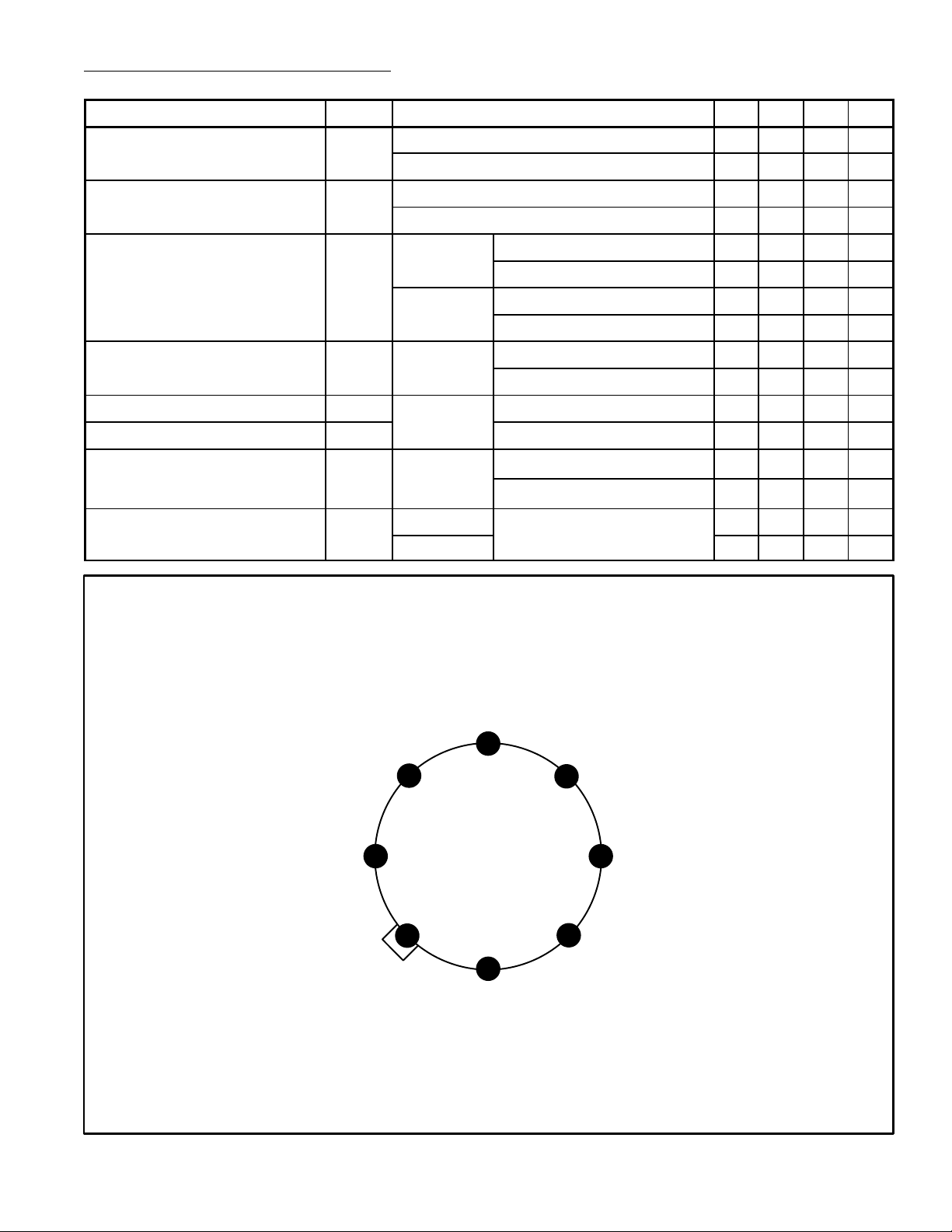
Pin Connection Diagram
(Top View)
Input Low
5
6
7
8
1
Input High
Current Source Emitter
4
Substrate and Case
3
2
Current Source Bias
 Loading...