

NTE NTE72 Datasheet
NTE72
Silicon NPN Transistor
High Current Amp, Fast Switch
Features:
D High Power: 100W @ TC = +50°C, VCE = 40V
D High Voltage: V
D High Current Saturation Voltage: V
D High Frequency: f
D Isolated Collector Package, No Isolating hardware Required
= 80V Min
CEO
= 30MHz Min
T
CE(sat)
= 1.5V @ 10A
Absolute Maximum Ratings:
Collector–Emitter Voltage, V
Collector–Emitter Voltage (Note 2), V
Emitter–Base Voltage, V
Collector Current, I
EBO
C
Total Power Dissipation (T
Operating Junction Temperature Range, T
Storage Temperature Range, T
Lead Temperature (During Soldering, 60sec max), T
(Note 1)
CES
CEO
= +50°C, VCE = 40V), P
C
opr
stg
100V. . . . . . . . . . . . . . . . . . . . . . . . . . . . . . . . . . . . . . . . . . . . . . . . . . . . .
80V. . . . . . . . . . . . . . . . . . . . . . . . . . . . . . . . . . . . . . . . . . . . . .
6V. . . . . . . . . . . . . . . . . . . . . . . . . . . . . . . . . . . . . . . . . . . . . . . . . . . . . . . . . .
10A. . . . . . . . . . . . . . . . . . . . . . . . . . . . . . . . . . . . . . . . . . . . . . . . . . . . . . . . . . . . . . . .
T
100W. . . . . . . . . . . . . . . . . . . . . . . . . . . . . . . . .
–65° to +200°C. . . . . . . . . . . . . . . . . . . . . . . . . . . . . . . .
–65° to +200°C. . . . . . . . . . . . . . . . . . . . . . . . . . . . . . . . . . . . . . . . . .
L
+300°C. . . . . . . . . . . . . . . . . . . . . . . . . . . . . . . .
Note 1. These ratings are limiting values above which the serviceability of the NTE72 transistor may
be impaired.
Note 2. This rating refers to a high current point where collector–emitter voltage is lowest.
Electrical Characteistics:
Parameter Symbol Test Conditions Min Typ Max Unit
Collector–Emitter Sustaining Voltage V
Collector–Emitter Breakdown Voltage V
Emitter–Base Breakdown Voltage V
DC Pulse Current Gain (Note 3) h
(TC = +25°C unless otherwise specified)
CEO(sus)IC
(BR)CES)IC
(BR)EBOIE
FE
= 200mA, IB = 0, Notes 2 & 3 80 – – V
= 1mA, VBE = 0 100 – – V
= 1mA, IC = 0 6 – – V
IC = 100mA, VCE = 5V 50 95 –
IC = 5A, VCE = 5V 70 108 200
IC = 5A, VCE = 5V, TC = –55°C 35 51 –
IC = 10A, VCE = 5V 45 91 –
Note 2. This rating refers to a high current point where collector–emitter voltage is lowest.
Note 3. Pulse Conditions: Pulse Width = 300µs, Duty Cycle = 1%.
Electrical Characteistics (Cont’d): (TC = +25°C unless otherwise specified)
Parameter Symbol Test Conditions Min Typ Max Unit
High Frequency Current Gain h
Collector–Emitter Saturation Voltage V
Base–Emitter Saturation Voltage V
Base–Emitter ON Voltage V
Collector Cutoff Current I
Collector Reverse Current I
Emitter Cutoff Current I
Collector–Base Capacitance C
CE(sat)IC
BE(sat)IC
BE(on)IC
CES
CEX
EBO
IC = 2A, VCE = 5V, f = 20MHz 2.0 2.8 –
fe
= 5A, IB = 0.5A, Note 3 – 0.55 0.9 V
IC = 10A, IB = 1A, Note 3 – 1.1 1.5 V
= 5A, IB = 0.5A, Note 3 – 1.2 1.8 V
IC = 10A, IB = 1A, Note 3 – 1.7 2.2 V
= 5A, VCE = 5V, Note 3 – – 1.8 V
VCE = 60V, VBE = 0 – 0.014 1.0 µA
VCE = 60V, VEB = 2V, TC = +150°C – – 500 µA
VEB = 5V, IC = 0 – – 1.0 µA
VCB = 10V, IE = 0, f = 1MHz – 235 275 pF
cb
Note 3. Pulse Conditions: Pulse Width = 300µs, Duty Cycle = 1%.
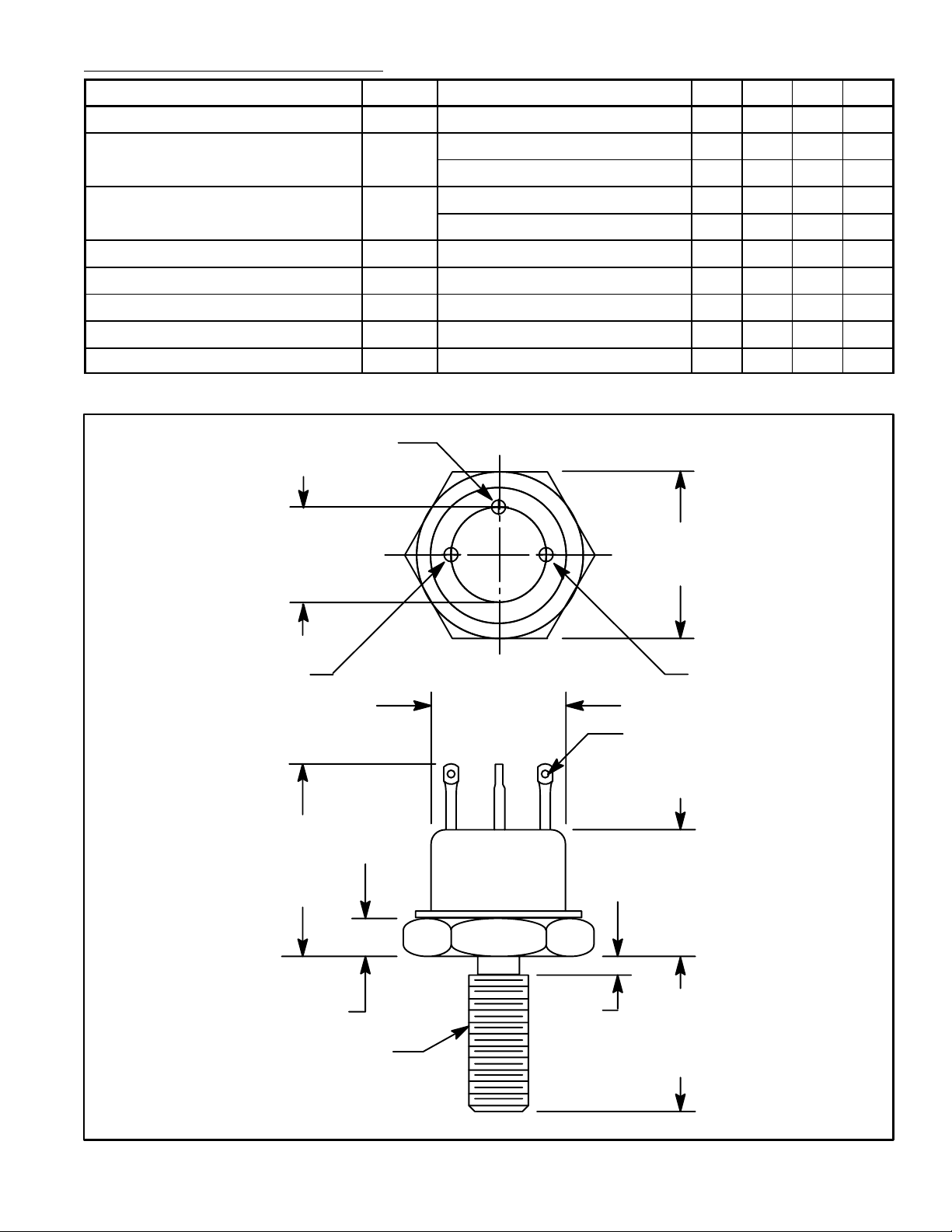
Base
.400
(10.16)
.682
(17.32)
Emitter Collector/
.600 (19.15)
Dia
.061 (1.53) Dia
Isolated Stud
.755
(19.15)
.412
(10.44)
.090 (2.28) Max
1/4–28 UNF–2A
.115
(2.93)
.440
(11.17)
 Loading...