

NTE NTE7158 Datasheet
NTE7158
Integrated Circuit
Deflection Circuit Power Amp for Color TV
Description:
The NTE7158 is an integrated circuit in a 7–Lead SIP type package designed for use as a power
amplifier for driving a deflection circuit in large and medium screen size color televisions.
Features:
D Large Output Current: 2.2A
D Small Power Dissipation with a Pump–Up Circuit
Absolute Maximum Ratings: (TA = +25°C unless otherwise specified)
Power Supply Voltage, V
CC
Pump–Up Power Supply Voltage, V
Terminal Voltage, E
Input Signal Voltage, e
Deflection Current (Note 1), i
in
in
d
Operating Temperature Range, T
Storage Temperature Range, T
P–P
stg
Max
opr
Vt
30V. . . . . . . . . . . . . . . . . . . . . . . . . . . . . . . . . . . . . . . . . . . . . . . . . . . . . . . . . .
60V. . . . . . . . . . . . . . . . . . . . . . . . . . . . . . . . . . . . . . . . . . . . . . . . .
GND–0.3V to VVt+0.3V. . . . . . . . . . . . . . . . . . . . . . . . . . . . . . . . . . . . . . . . . . . . . . .
0V to 1.2V. . . . . . . . . . . . . . . . . . . . . . . . . . . . . . . . . . . . . . . . . . . . . . . . . . . . . . .
±1.5A. . . . . . . . . . . . . . . . . . . . . . . . . . . . . . . . . . . . . . . . . . . . . . . . . . . . . .
–20° to +85°C. . . . . . . . . . . . . . . . . . . . . . . . . . . . . . . . . . . . . . . . .
–55° to +150°C. . . . . . . . . . . . . . . . . . . . . . . . . . . . . . . . . . . . . . . . . .
Note 1. Power on time: 2ms, V
CEO
= 60V.
Note 2. Using an infinite heat sink.
Recommended Operating Conditions:
Parameter Symbol Test Conditions Min Typ Max Unit
Power Supply V
Deflection Output Current I
CC
2P–P
– 27 29 V
– – 2.2 A
Electrical Characteristics: (VCC = 24V, TA = +25°C unless otherwise specified)
Parameter Symbol Test Conditions Min Typ Max Unit
Saturation Voltage of the Vertical Output Transistor V
Saturation Voltage of the Pump–Up Output Transistor V
Output Current with No Input I
Center Output Voltage V
1 Note 3 0.3 0.5 1.0 V
V(sat)
V
2 Note 4 1.0 1.8 3.6 V
V(sat)
1 Note 5 1.0 2.0 3.0 V
P(sat)
V
2 Note 6 0.2 0.8 1.6 V
P(sat)
Note 7 – 26 – mA
b
center
10 12 14 V
P–P
Notes:
Note 3. SW1: ON, SW2: C, SW3: ON, SW4: B, SW5: A, SW6: A
Measure the voltage of Pin2.
Note 4. SW
Note 5. SW
Note 6. SW
: ON, SW2: C, SW3: ON, SW4: A, SW5: A, SW6: B
1
Measure the voltage of Pin2, V
: ON, SW2: B, SW3: OFF, SW4: A, SW5: C, SW6: A
1
Measure the voltage of Pin7, V
: OFF, SW2: C, SW3: OFF, SW4: A, SW5: B, SW6: B
1
2
7
. V
. V
2 = VCC–V2.
V(sat)
1 = VCC–V7.
P(sat)
Measure the voltage of Pin7.
Note 7. SW
: ON, SW2: A, SW3: ON, SW4: C, SW5: A, SW6: B
1
Measure the sink current into Pin3. Measure the voltage of Pin2.
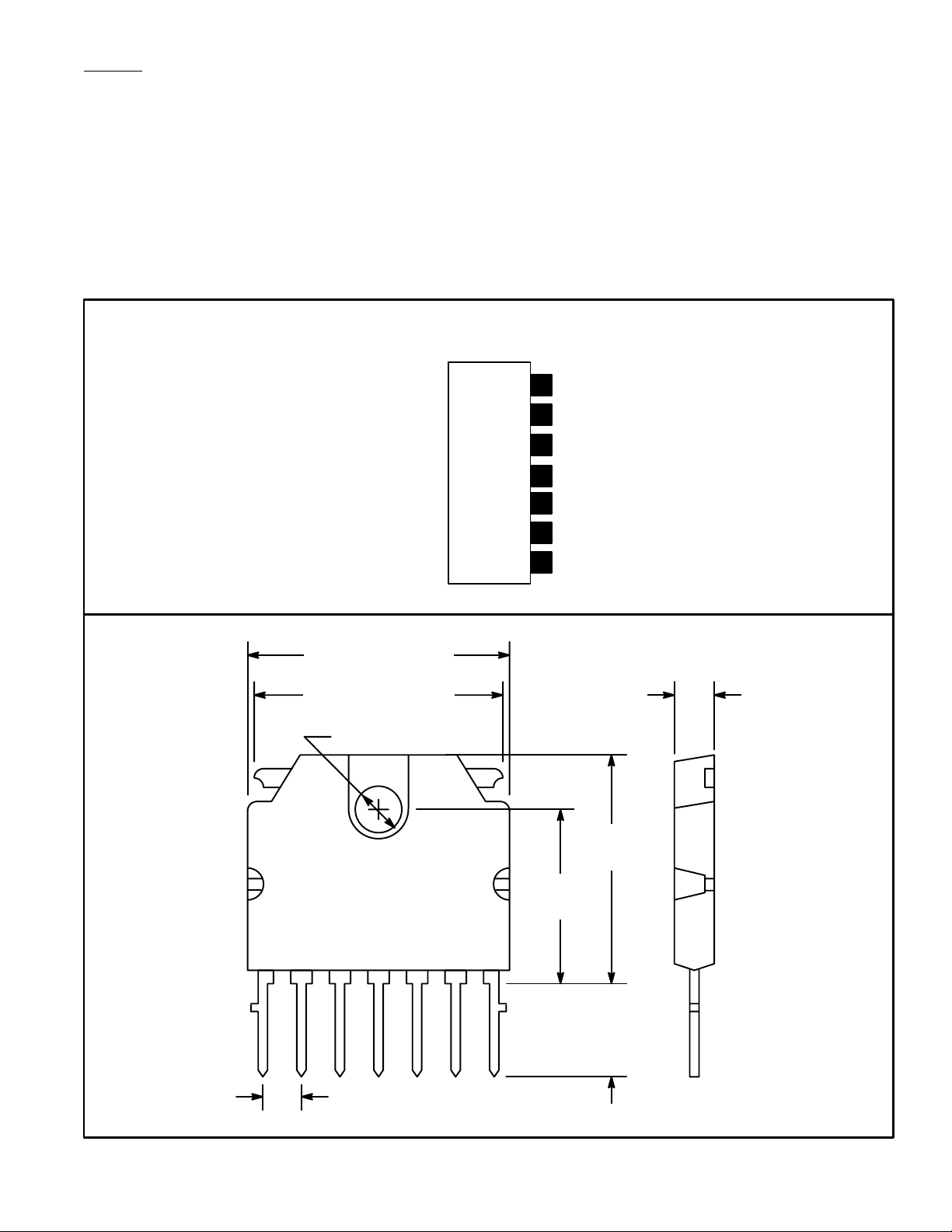
Pin Connection Diagram
(Front View)
7
Pump–Up Output
6
V
CC
5
Phase Compensation
4
Input
Pump–Up Power Supply
3
2
Vertical Output
1
GND
.681 (17.3) Max
.641 (16.3) Max
.118 (3.0)
.125 (3.2) Dia
.638
(16.2)
.504
(12.8)
17
.100 (2.54)
.209
(5.5)
Min
 Loading...