

NTE NTE7153 Datasheet
NTE7153
Integrated Circuit
Vertical Deflection Output Circuit
Description:
The NTE7153 is a vertical deflection output integrated circuit in a 7–Lead SIP type package designed
for use in TV and CRT displays with excellent image quality that use a BUS control system signal processing IC. This device can drive the direct (even including a DC component) deflection yoke with the
sawtooth wave output from the BUS control system signal processing IC. Because the maximum
deflection current is 2.2A
Features:
D Low Power Dissipation due to Built–In Pump–Up Circuit
D Vertical Output Circuit
D Thermal Protection Circuit Built–In
D Excellent Crossover Characteristics
D DC Coupling Possible
, the NTE7153 is suitable for use in large screen sets.
P–P
Absolute Maximum Ratings:
(TA = +25°C unless otherwise specified)
Maximum Supply Voltage, VCC6 max 34V. . . . . . . . . . . . . . . . . . . . . . . . . . . . . . . . . . . . . . . . . . . . . . . . .
Output Block Supply Voltage, V
Deflection Output Current, I
2
Allowable Power Dissipation (With Arbitraily Large Heat Sink), P
Operating Temperature Range, T
Storage Temperature Range, T
Thermal Resistance, Junction–to–Case, R
Recommended Operation Conditions:
Parameter Symbol Test Conditions Min Typ Max Unit
Recommended Supply Voltage VCC6 – 24 – V
Operating Supply Voltage Range VCC6 op 16 – 33 V
Recommended Deflection Output Current I
3 max 70V. . . . . . . . . . . . . . . . . . . . . . . . . . . . . . . . . . . . . . . . . . . . . .
CC
max –1.5 to +1.5A
. . . . . . . . . . . . . . . . . . . . . . . . . . . . . . . . . . . . . . . . .
max 9W. . . . . . . . . . . . . . . . . . . .
D
opr
stgv
thJC
–20° to +85°C. . . . . . . . . . . . . . . . . . . . . . . . . . . . . . . . . . . . . . . . .
–40° to +150°C. . . . . . . . . . . . . . . . . . . . . . . . . . . . . . . . . . . . . . . . . .
4°C/W. . . . . . . . . . . . . . . . . . . . . . . . . . . . . . . . . . . . . . .
(TA = +25°C unless otherwise specified)
2P–P
– – 2.2 A
P–O
P–P
Electrical Characteristics: (VCC6 = 24V, TA = +25°C unless otherwise specified)
Parameter Symbol Test Conditions Min Typ Max Unit
Pump–Up Charge Saturation Voltage VS7–1 I7 = 20mA – – 1.8 V
Pump–Up Discharge Saturation Voltage VS6–7 I7 = –1.1A – – 3.2 V
Deflection Output Saturation Voltage (Lower) VS2–1 I2 = 1.1A – – 1.5 V
Deflection Output Saturation Voltage (Upper) VS3–2 I2 = –1.1A – – 3.5 V
Idling Current I
Midpoint Voltage V
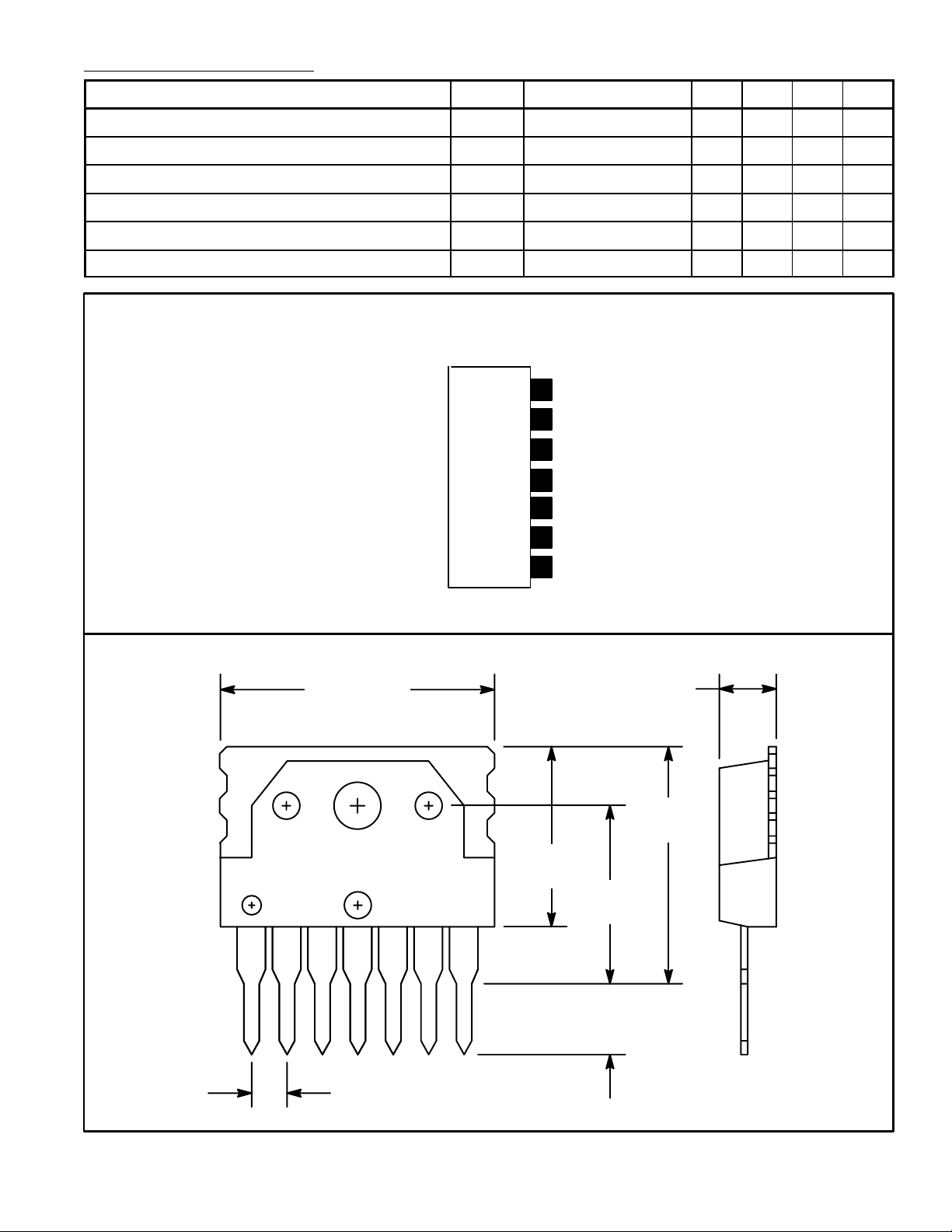
Pin Connection Diagram
(Front View)
DL
MID
Pump–Up Output
7
6
V
CC
Inverting Input
5
4
Non–Inverting Input
Output Stage V
3
Ver. Output
2
1
GND
35 – 65 mA
11 12 13 V
CC
.708 (18.0)
.118 (3.0)
.590
(15.0)
.527
(13.4)
.425
(10.8)
17
.228
(5.8)
.100 (2.54)
 Loading...