

NTE NTE7151 Datasheet
NTE7151
Integrated Circuit
I2C Bus Control NTSC 1–Chip Color TV IC
Description:
The NTE7151 is an integrated circuit in a 56–Lead DIP type package designed for use as a PIF, SIF,
video, chroma and deflection circuit for NTSC color TVs. This device also provides audio/video
switching and a text interface.
Features:
PIF Circuit
D PLL Type IF Demodulation (Bus Alignment)
D Adjustment Free AFT Without Tank Coil
Video Circuit
D Black Stretcher
D DC Restoration Circuit
D D.L. Aperture Compensate Circuit (Bus Control)
D Internal Filter Auto–Adjust Circuit (FSC Link Type)
Chroma Circuit
D Color Control Circuit (Bus Control)
D Tint Control Circuit (Bus Control)
D RF AGC Output (Delay Point: Bus Alignment)
D Dual Time Constant Fast AGC
D Uni–Color Circuit (Bus Control)
D 3.58MHz Trap Filter Circuit (Bus ON/OFF)
D Y Delay Line Circuit
D B.P.F. / T.O.F. Circuit (Bus Select)
D Included ACC/Killer Filter
SIF Circuit
D Inter Carrier SIF System
D External Sound Select Switch (Bus Select)
Text Circuit
D Linear RGB Input
D Cut Off/Drive Adjustment (Bus Adjustment)
Deflection Circuit
D Adjustment Free Countdown System
D Sync. Separation Output
D X–Ray Protect Circuit
D Auto–Slicer Type High Performance Sync. Separation Circuit
D Horizontal and Vertical Position Adjustment (Bus Adjustment)
D Attenuator Circuit (Bus Control)
D RGB Primary Color Output
D Vertical Amplitude Adjustment (Bus Adjustment)
D Vertical Ramp Output
D Dual Time Constant AFC Circuit
Absolute Maximum Ratings: (TA = +25°C unless otherwise specified)
Power Supply Voltage, V
CC
Power Dissipation, PDmax 2.19W. . . . . . . . . . . . . . . . . . . . . . . . . . . . . . . . . . . . . . . . . . . . . . . . . . . . . . . . .
Derate Above 25°C 17.5mW/°C. . . . . . . . . . . . . . . . . . . . . . . . . . . . . . . . . . . . . . . . . . . . . . . . . . . .
Input Terminal Voltage, V
Input Signal Amplitude, e
in
. . . . . . . . . . . . . . . . . . . . . . . . . . . . . . . . . . . . . . . . . . . . . . . . . . . . . . . .
in
Operating Temperature Range, T
Storage Temperature Range, T
stg
opr
GND–0.3V to VCC+0.3V. . . . . . . . . . . . . . . . . . . . . . . . . . . . . . . . . . . . . . . .
–20° to +65°C. . . . . . . . . . . . . . . . . . . . . . . . . . . . . . . . . . . . . . . . .
–55° to +150°C. . . . . . . . . . . . . . . . . . . . . . . . . . . . . . . . . . . . . . . . . .
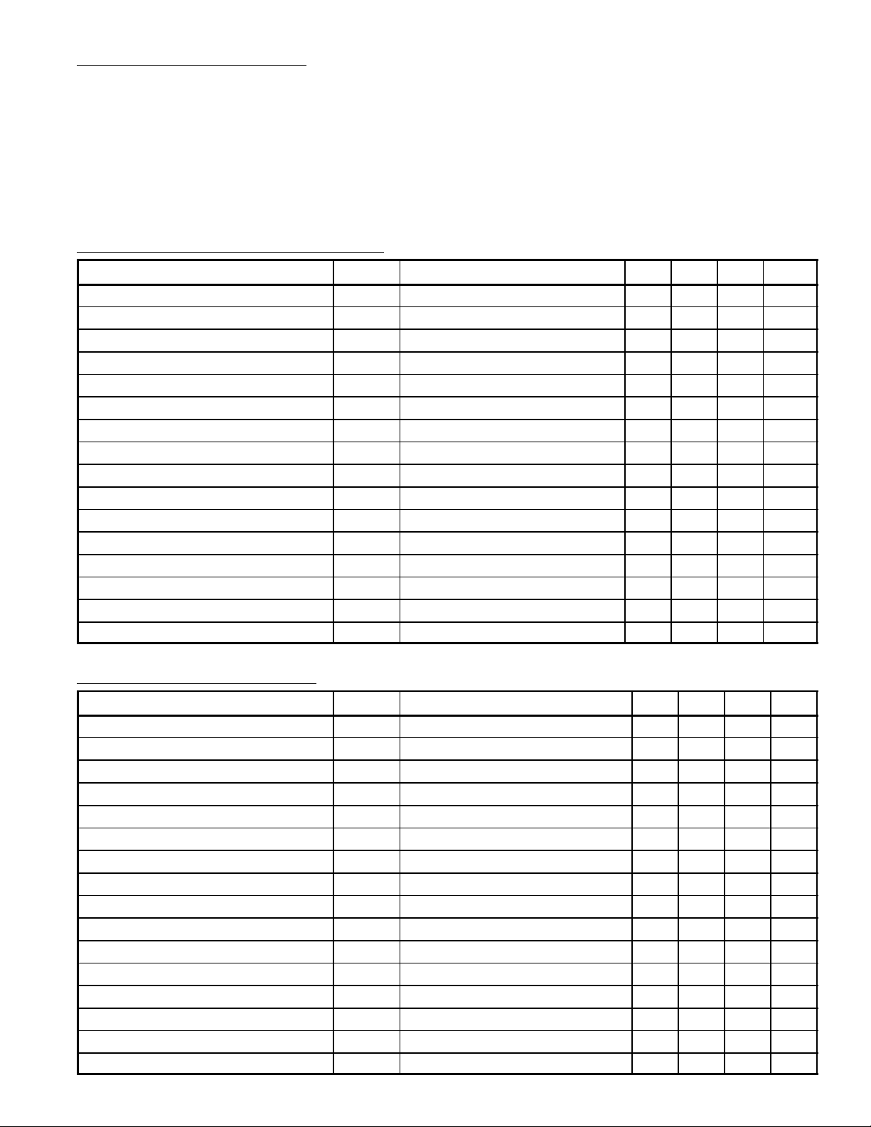
Recommended Operating Conditions:
Parameter Symbol Test Conditions Min Typ Max Unit
PIF Power Supply Voltage V
SIF Power Supply Voltage V
V/C/D Power Supply Voltage V
CCP
CCS
CCV
H. VCC Power Supply Voltage H. V
D. VCC Power Supply Voltage D. V
TV External Video Input Level V
Standard Video Input Level V
Standard Chroma Input Level V
FBP Width T
FBP Input Flow In Current I
in37/39
in43
in45
FBP
FBP
PIF Output Load Resistor R
SIF Output Load Resistor R
RGB Output Load Resistor R
Horizontal Output Load Resistor R
Vertical Output Load Resistor R
Sync.Separation Output Flow In Current I
ORGB
HOUT
VOUT
sync
CC
CC
Including Sync. – 1.0 – V
Including Sync. – 1.0 – V
At Burst Signal – 286 – mV
Vth = 1.4V, VCC = –1.4V 10 12 – µs
max – – 2 mA
OP
OS
maximum 10mA 330 800 – Ω
max – – 1 mA
8.5 9.0 9.5 V
8.5 9.0 9.5 V
8.5 9.0 9.5 V
8.5 9.0 9.5 V
2.7 3.3 3.8 V
2.0 8.2 – kΩ
1.0 8.2 – kΩ
– 1.8 – kΩ
4.1 5.7 – kΩ
4V
12V. . . . . . . . . . . . . . . . . . . . . . . . . . . . . . . . . . . . . . . . . . . . . . . . . . . . . . . . . .
P–P
P–P
P–P
P–P
DC Electrical Characteristics: (VCC = 9V, H. VCC = 9V, TA = +25°C unless otherwise specified)
Parameter Symbol Test Conditions Min Typ Max Unit
Sound Output (Pin1) V
Sound Output (Pin2) V
RF AGC (Pin3) V
AGC Filter (Pin5) V
1
2
3
5
PIF GND (Pin6) GND – 0.0 – V
PIF Input (Pin7) V
PIF Input (Pin8) V
PIF VCC (Pin9) V
Loop Filter (Pin10) V
APC Filter (Pin11) V
VCXO (Pin12) V
7
8
CC
10
11
12
V/C/D GND (Pin13) GND – 0.0 – V
F–BLK (Pin14) V
Analog R Input (Pin15) V
Analog G Input (Pin16) V
Analog B Input (Pin17) V
14
15
16
17
3.2 3.7 4.2 V
3.2 3.7 4.2 V
– 0.0 0.5 V
7.0 7.5 8.0 V
1.5 2.0 2.5 V
– 0.0 0.5 V
– 9.0 – V
– 4.5 – V
6.0 6.5 7.0 V
5.3 5.8 6.3 V
– 0.0 – V
4.4 4.9 5.4 V
4.4 4.9 5.4 V
4.4 4.9 5.4 V
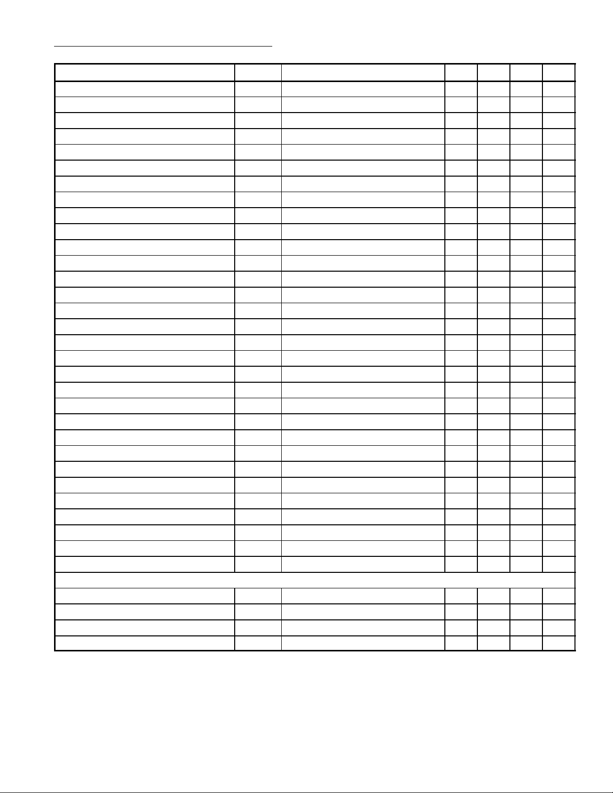
DC Electrical Characteristics (Cont’d): (VCC = 9V, H. VCC = 9V, TA = +25°C unless otherwise
specified)
Parameter Symbol Test Conditions Min Typ Max Unit
D. VCC (Pin18) V
R Output (Pin19) V
G Output (Pin20) V
B Output (Pin21) V
V SEPA (Pin25) V
H. VCC (Pin26) V
SCL (Pin27) V
SDA (Pin28) V
X–RAY (Pin29) V
H. AFC (Pin33) V
32fH VCO (Pin34) V
CC
BRT, C.O Cent 2.4 2.7 2.9 V
19
BRT, C.O Cent 2.4 2.7 2.9 V
20
BRT, C.O Cent 2.4 2.7 2.9 V
21
25
26
27
28
29
33
34
D. GND (Pin35) GND – 0.0 – V
ABL (Pin36) V
TV Input (Pin37) V
ACL (Pin38) V
EXT. Video Input (Pin39) V
Black DET (Pin40) V
AV/SW Output (Pin41) V
DC Rest (Pin42) V
Y Input (Pin43) V
AFT (Pin44) V
Chroma Input (PIn45) V
V / C / D VCC (Pin46) V
TV DET. Output (Pin47) V
SIF VCC (Pin48) V
BRT, COL Cent 2.9 3.4 3.9 V
36
37
BRT, COL Cent 2.9 3.4 3.9 V
38
39
40
41
42
43
44
45
46
47
CC
SIF GND (Pin51) GND – 0.0 – V
Limiter Input (Pin52) V
Audio TV Input (Pin53) V
De–Emphasis (Pin54) V
EXT. Audio Input (Pin55) V
EXT. Audio Input (Pin56) V
52
53
Pin4 GND 4.0 4.5 5.0 V
54
55
55
Current Consumption
IF Power Supply Current I
V / C / D Power Supply Current I
H. VCC Power Supply Current I
D. VCC Power Supply Current I
cci
ccv
cch
ccd
– 3.3 – V
5.8 6.3 6.8 V
– 9.0 – V
4.5 5.0 5.5 V
4.5 5.0 5.5 V
– 0.0 – V
7.0 7.5 8.0 V
5.5 6.0 6.5 V
2.9 3.0 3.9 V
1.1 1.6 2.1 V
6.1 6.6 7.1 V
1.8 2.3 2.8 V
5.5 6.0 6.5 V
4.0 4.5 5.0 V
2.0 2.5 3.0 V
1.6 1.85 2.1 V
– 9.0 – V
4.7 5.2 5.7 V
– 9.0 – V
– 0.0 0.5 V
2.5 3.0 3.5 V
2.5 3.0 3.5 V
2.5 3.0 3.5 V
32.8 46.0 52.0 mA
52.7 71.0 76.8 mA
10.7 14.0 18.4 mA
5.2 10.0 11.6 mA
 Loading...