

NTE NTE7150 Datasheet
NTE7150
Integrated Circuit
Video, Chroma, and Sync. Signal Processing Circuit
for PAL/NTSC/SECAM System Color Televisions
Description:
The NTE7150 is an integrated circuit in a 64–Lead SIP type package designed for PAL/NTSC/SECAM
system color televisions involving video, chroma, and sync. signal processing circuits.
The video section contains a high–performance picture quality emphasis circuit, the chroma section
contains a PAL/NTSC/SECAM system automatic identification circuit, and the sync. section contains
a 50/60Hz automatic identification circuit. The PAL/SECAM demodulating circuit uses a baseband
signal processing system, providing an adjustment–free demodulating circuit. User control functions,
system switching, etc. are controlled via the I2C bus.
Features:
Video Section
D Sharpness Control with Internal Delay Lines
D Black Stretching Circuit
D YNR
D Variable DC Restoration Ratio
D Gamma (g) Contrast Correction
Chroma Section
D PAL/SECAM baseband Demodulation System
D Automatic Srystal Frequency Identification (4.43MHz/3.58MHz/M, N–PAL)
D Automatic Chroma System Identification (PAL/NTSC/SECAM)
D PLL SECAM Adjustment–Free Demodulation Circuit without and Tank Coils
D Built–In SECAM BELL Filter
Sync. Section
D Adjnustment–Free Horizontal and Vertical Oscillation Circuits based on Countdown System
D Automatic Vertical Frequency Identification (50/60Hz)
Absolute Maximum Ratings: (TA = +25°C unless otherwise specified)
Supply Voltage, V
CC
Power Dissipation, PDmax 2660mW. . . . . . . . . . . . . . . . . . . . . . . . . . . . . . . . . . . . . . . . . . . . . . . . . . . . . .
Derate Above 25°C 21.2mW/°C. . . . . . . . . . . . . . . . . . . . . . . . . . . . . . . . . . . . . . . . . . . . . . . . . . . .
Input Signal Amplitude, e
Applied Voltage, E
in
Operating Temperature Range, T
Storage Temperature Range, T
. . . . . . . . . . . . . . . . . . . . . . . . . . . . . . . . . . . . . . . . . . . . . . . . . . . . . . . .
in
GND–0.3V to VCC+0.3V. . . . . . . . . . . . . . . . . . . . . . . . . . . . . . . . . . . . . . . . . . . . . .
opr
stg
–55° to +150°C. . . . . . . . . . . . . . . . . . . . . . . . . . . . . . . . . . . . . . . . . .
–20° to +65°C. . . . . . . . . . . . . . . . . . . . . . . . . . . . . . . . . . . . . . . . .
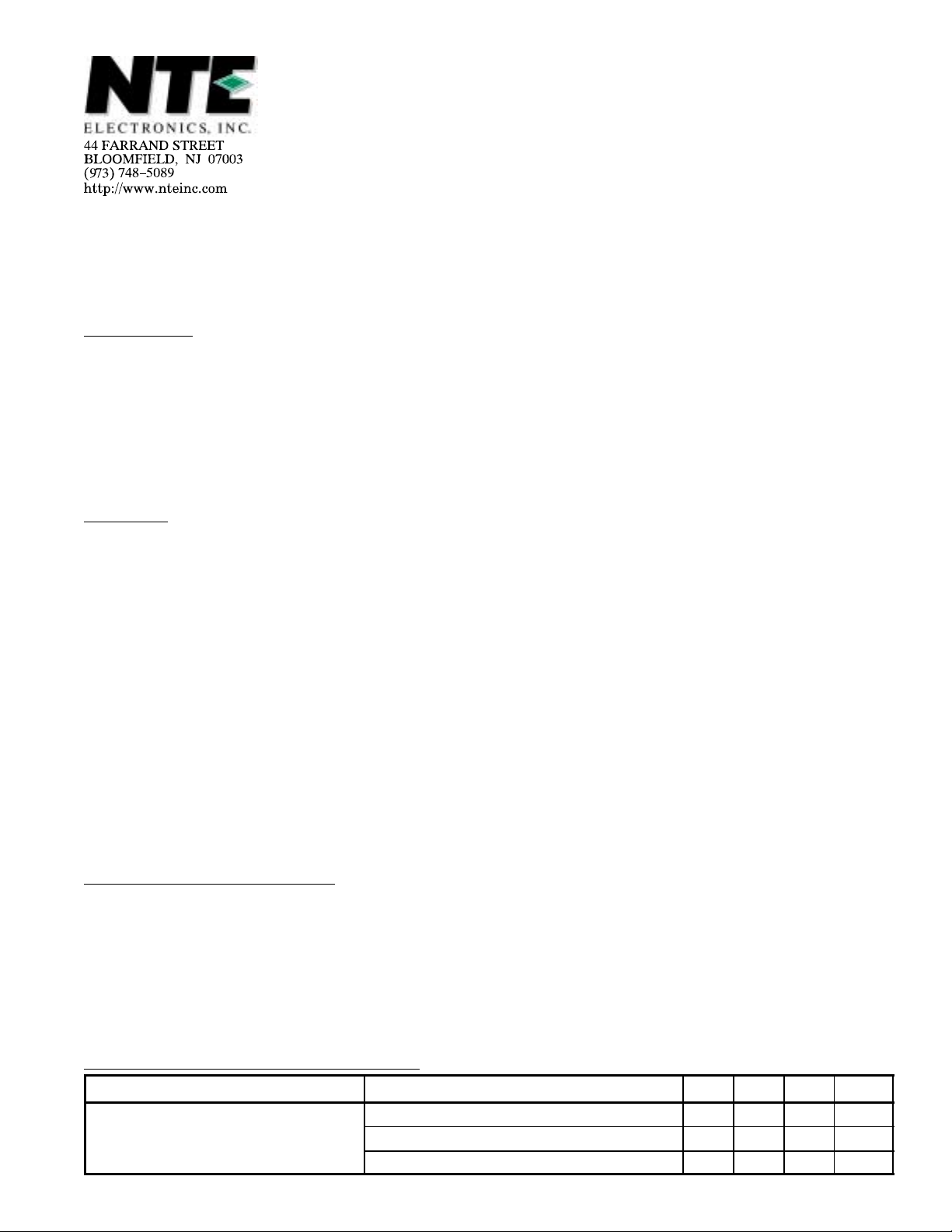
Recommended Operating Conditions:
Parameter Test Conditions Min Typ Max Unit
Supply Voltage At Pin19, Pin36, Pin50, and Pin59 8.1 9.0 9.5 V
At Pin5 8.1 9.0 10.0 V
At Pin4 3.0 3.3 3.6 V
5V
15V. . . . . . . . . . . . . . . . . . . . . . . . . . . . . . . . . . . . . . . . . . . . . . . . . . . . . . . . . . . . . . . .
P–P
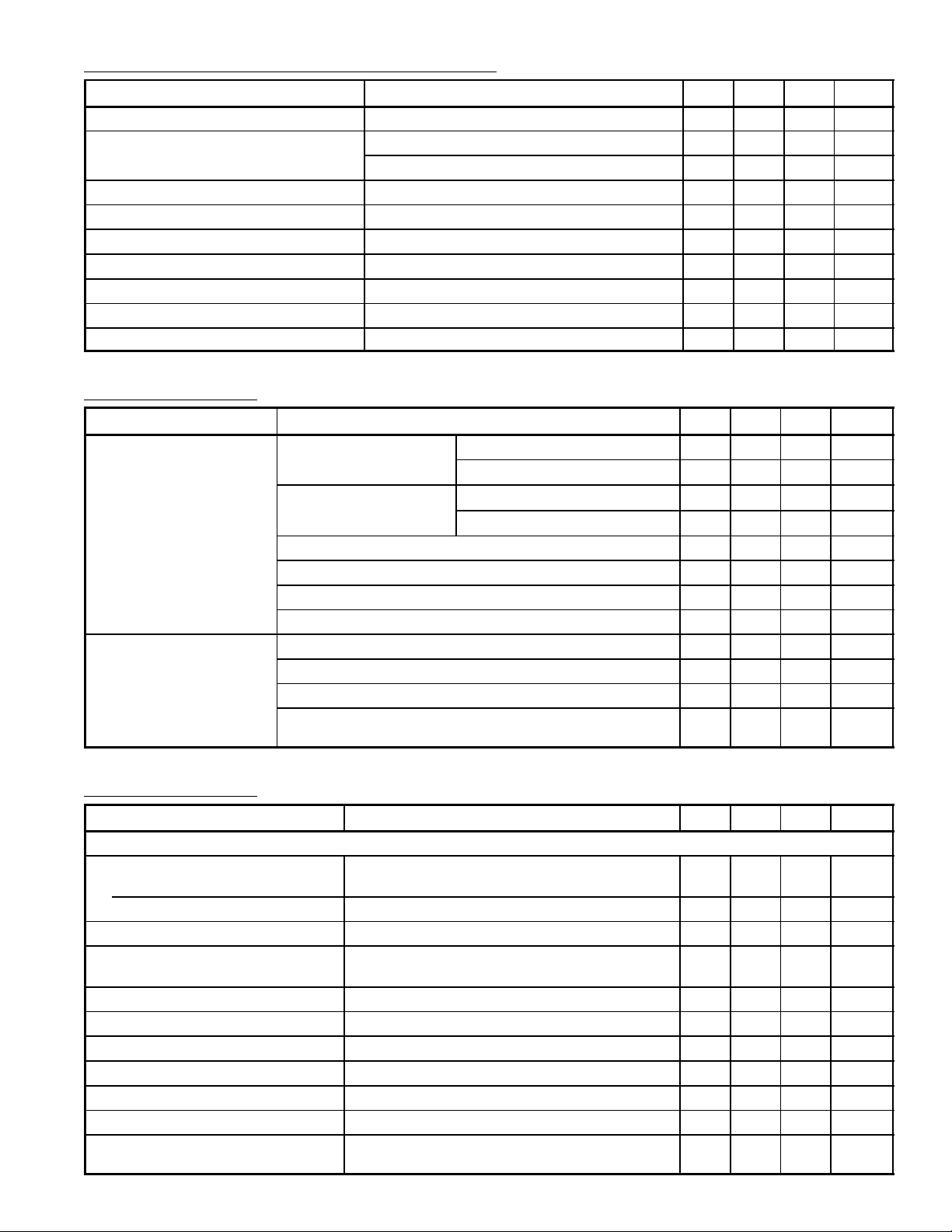
Recommended Operating Conditions (Cont’d):
Parameter Test Conditions Min Typ Max Unit
Video Input Signal Level Composite Video Signal Amplitude 0.7 1.0 1.2 V
Chroma Input Signal Level PAL/NTSC Chroma Input 100 200 300 mV
SECAM Chroma Input 50 100 150 mV
Sync Input Signal Level Composite Video Signal Amplitude 1.0 2.0 2.5 V
Text Input Signal Level 0.5 0.7 1.0 V
FBP Width 11 12 13 µs
FBP Input Current 0.3 1.0 1.3 mA
RGB Output Current – 1.0 2.0 mA
H. Out Output Current – 3.0 5.0 mA
VP Output Current – 1.0 2.0 mA
DC Characteristics: VCC = 9V, Logic VCC = 3.3V, TA = +25°C unless otherwise specified)
Parameter Test Conditions Min Typ Max Unit
Supply Current
Logic VCC (Pin4) = 3.3V
Video/Chroma VCC Turned OFF 15 30 40 mA
H. VCC (Pin5) = 9V
Video/Chroma VCC Turned OFF 15 30 40 mA
TEXT Section VCC (Pin19) = 9V 15 31 44 mA
SECAM Section VCC (Pin36) = 9V 10 18 25 mA
Chroma Section VCC (Pin50) = 9V 12 27 38 mA
Video Section VCC (Pin59) = 9V 17 37 52 mA
Terminal Voltage Pin2 7.2 7.4 7.8 V
Pin16, Pin17, and Pin18 (In Mute Mode) 1.7 2.0 2.3 V
Pin22, Pin23, and Pin24 (Uni–Color DAC center) 3.3 3.8 4.2 V
Pin63 (Apply 5V with 5.1kΩ Resistor, Measure DC Output
Voltage at T race Period)
10 20 28 mA
10 20 28 mA
3.1 3.5 3.9 V
P–P
P–P
P–P
P–P
P–P
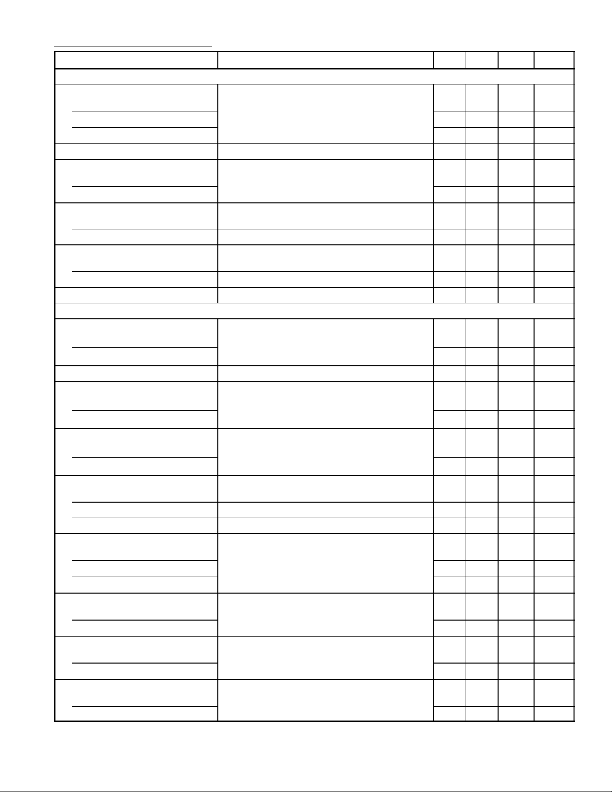
AC Characteristics: VCC = 9V, Logic VCC = 3.3V, TA = +25°C unless otherwise specified)
Parameter Test Conditions Min Typ Max Unit
Video Section
Y Input Dynamic Range
Upper Measure dynamic range above the pedestal level 0.7 1.0 1.3 V
Lower Measure dynamic range below the pedestal level 0.0 0.3 0.5 V
Y Input Impedance Measure input impedance of Pin60 100 130 – kΩ
Y Input Clamp Voltage Measure DC voltage at Pin60 when Y input
connected to AC GND.
Maximum Y Gain 15.0 17.5 23.0 dB
Y Frequency Bandwidth 8 10 15 MHz
Black Stretching Amp Maximum Gain 1.3 1.4 1.5
Black Stretching Start Point 40 50 65 IRE
DC Restoration Ratio 97 100 103 %
Black Stretching Start Voltage 3.2 3.3 3.6 V
Delay Time of Sharpness Circuit Measure difference in Y output signal delay time
between sharpness SW turned ON and OFF.
2.5 2.8 3.1 V
115 125 135 ns
P–P
P–P
AC Characteristics (Cont’d): VCC = 9V, Logic VCC = 3.3V, TA = +25°C unless otherwise specified)
Parameter Test Conditions Min Typ Max Unit
Video Section (Cont’d)
Sharpness Control
Maximum Gain
Center Gain
Minumim Gain
Input 2T pulse VBS to TP60 and TP63. Measure
2T pulse output gain of data = 3FH, 20H, and
00H. 0dB is equal to the output gain of sharpness
00H. 0dB is equal to the output gain of sharpness
SW OFF.
YNR Gain –20 –13 –8 dB
Contact Control
Center Gain
Minimum Gain
Measure Y output gain of data = 40H and 00H.
Maximum Y gain is 0dB.
g Point
V
a
V
b
g Gain
G
a
G
b
Y Signal to Noise Ratio 50 55 60 dB
Chroma Section 1 (PAL/NTSC)
ACC Output Characteristics
e300
e100
Input rainbow signal whose burst and chroma
signal level is 300mV
and 100mV
P–P
P–P
.
Measure sugnal amplitude at Pin41.
ACC Flatness 3300/e100 0.9 1.0 1.1
Killer–On Level
PAL
NTSC
Input color bar signal. Measure burst amplitude
at which color begins to disappear when burst is
gradually reduced.
Killer–Off Level
PAL
NTSC
Input color bar signal. Measure burst amplitude
at which color begins to be tinted when burst is
gradually increased from 0.
APC Pull–In Range
3.58MHz fo = 3.579545MHz ±300 ±500 ±1000 Hz
4.43MHz fo = 4.433619MHz ±300 ±500 ±1000 Hz
M PAL fo = 3.575611MHz ±300 ±500 ±1000 Hz
VCXO Freq Control Sensitivity
4.43MHz
3.58MHz
Fix X–tal mode with bus. Measure frequency
changes at TP28 when varying TP26 voltage
from 6.2V to 6.3V.
from 6.2V to 6.3V.
M PAL
fsc Output Amplitude
4.43MHz
3.58MHz
Fix X’tal mode with bus. Measure signal
amplitude at TP28.
fsc Output Voltage
4.43MHz
3.58MHz
Fix X’tal mode with bus. Measure DC voltage at
TP28.
B–Y Output Amplitude
4PAL
3NTSC
Input rainbow signal. Measure signal amplitude
at Pin41.
3.5 5.5 7.5 dB
0.5 1.5 3.5 dB
–3 –1 +1 dB
–4.0 –5.5 –7.0 dB
–17 –19 –21 dB
40 50 60 IRE
80 90 100 IRE
–1 –3 –5 dB
–4 –6 –8 dB
260 370 520 mV
260 370 520 mV
0.2 0.5 1.0 mV
0.2 0.5 1.0 mV
1.0 2.5 4.0 mV
1.0 2.5 4.0 mV
P–P
P–P
P–P
P–P
P–P
P–P
1.7 2.4 3.2 Hz/mV
1.5 2.2 3.0 Hz/mV
1.8 2.5 3.3 Hz/mV
130 150 170 mV
120 140 160 mV
P–P
P–P
3.6 3.9 4.2 V
2.8 3.1 3.4
260 370 520 mV
260 370 520 mV
V
P–P
P–P
 Loading...