

NTE NTE7148 Datasheet
NTE7148
Integrated Circuit
Color TV Single–Chip Signal Processor
for NTSC Systems (PLL Detection)
Description:
The NTE7148 is an integrated circuit in a 52–Lead DIP type package designed for use in color TVs
based on the NTSC (National Television System Committee) system with an on–chip circuit for all VIF,
SIF, video, chroma, and deflection signal processing.
Functions and Features:
VIF
D PLL Detection (High Video and Audio Quality)
D High–Gain VIF Amplifier
SIF
D Simultaneous Sound IN/OUT
D Video/Audio Simultaneous Muting, or Audio–Only Muting Possible
Audio–Visual Switch
D Internal/External Audio–Visual Switch (VCC = 9V)
Delay Line Video External, Audio External Switch Rating
OFF IN 6.9V to 9.0V
OFF EXT 4.7V to 6.6V
ON EXT 2.4V to 4.3V
ON IN 0V to 2.1V
D High Speed AGC
D On–Chip APC Time Constant Switch
OSD
D RGB 3 Input
D RGB Linear Amplifier (–6dB Input: 2V to 5V)
Chroma
D On–Chip ACC Filter
D On–Chip Killer Filter
Video
D Black Enhancement
D DC Playback
D On–Chip Delay Line
D Wideband Width (9MHz): Delay Line Short
Deflection
D Adjustment–Free Horizontal, Vertical Synchronization
D Dual AFC System with Excellent Anti–Noise Characteristics
D External Adjustmant of Vertical Synchronization Sensitivity
D Vertical Size is Constant with No–Signal
D Highly Stable Image During Playback of Copy Protected tapes (Macro–Vision Tape etc.)
D High Stability Against VCR Skew Distortion
D Fast Blanking (B Input Combined Use)
D Killer–Circuit Hysteresis Operation
D On–Chip Carrier Filter
D Dual Rank On–Chip Differential Circuit Also
Available for Soft Also
D S Input Supported (VCR Application)
D Variable DC Transmission Volume Available
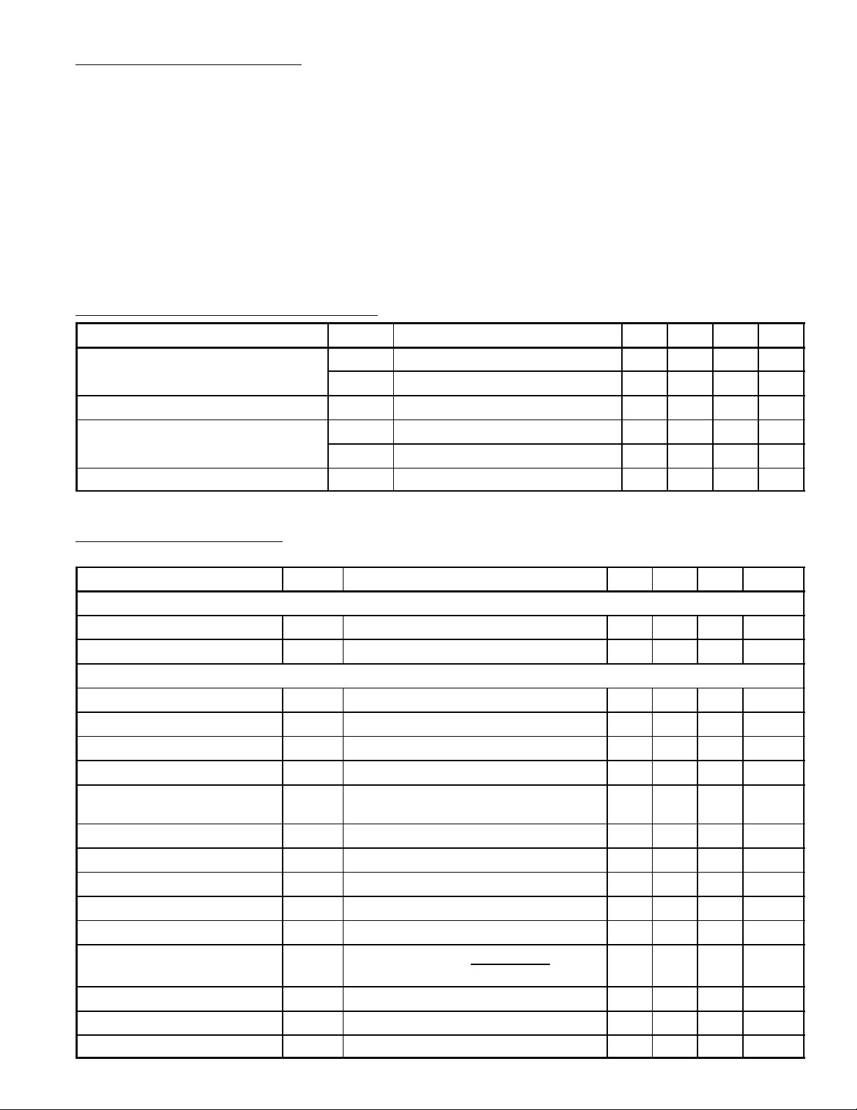
Absolute Maximum Ratings: (TA = +25°C unless otherwise specified)
Maximum Supply Voltage, V11max 11V. . . . . . . . . . . . . . . . . . . . . . . . . . . . . . . . . . . . . . . . . . . . . . . . . . . .
Maximum Supply Voltage, V14max 11V. . . . . . . . . . . . . . . . . . . . . . . . . . . . . . . . . . . . . . . . . . . . . . . . . . .
Maximum Supply Current, I30max 16mA. . . . . . . . . . . . . . . . . . . . . . . . . . . . . . . . . . . . . . . . . . . . . . . . . .
Circuit Current, I
Circuit Current, I
44
6
FBP Input Current (Peak Current), I22max 5mA. . . . . . . . . . . . . . . . . . . . . . . . . . . . . . . . . . . . . . . . . . . .
FBP Input Current (Peak Current), I21max 10mA. . . . . . . . . . . . . . . . . . . . . . . . . . . . . . . . . . . . . . . . . . .
Allowable Power Dissipation (TA ≤ +60°C), PDmax 1.35W. . . . . . . . . . . . . . . . . . . . . . . . . . . . . . . . . . . .
Operating Temperature Range, T
Storage Temperature Range, T
stg
opr
–10° to +65°C. . . . . . . . . . . . . . . . . . . . . . . . . . . . . . . . . . . . . . . . .
–55° to +150°C. . . . . . . . . . . . . . . . . . . . . . . . . . . . . . . . . . . . . . . . . .
Recommended Operating Conditions: (TA = +25°C unless otherwise specified)
Parameter Symbol Test Conditions Min Typ Max Unit
–6mA. . . . . . . . . . . . . . . . . . . . . . . . . . . . . . . . . . . . . . . . . . . . . . . . . . . . . . . . . . . . . . . .
–3mA. . . . . . . . . . . . . . . . . . . . . . . . . . . . . . . . . . . . . . . . . . . . . . . . . . . . . . . . . . . . . . . . .
Supply Voltage V
Supply Current I
Operating Voltage Range V11op 8.0 – 9.5 V
Operating Current Range I30op 10 – 16 mA
11
V
14
30
V14op 8.0 – 9.5 V
– 9 – V
– 9 – V
– 13 – mA
Electrical Characteristics: (TA = +25°C, VCC = V11 = V14 = 9V, ICC = I30 = 13mA unless otherwise
specified)
Parameter Symbol Test Conditions Min Typ Max Unit
Circuit Voltage and Current
Horizontal Supply Voltage V
Supply Current I
VIF
Quiescent Video Output Voltage V
Quiescent AFT Output Voltage V
Maximum RF AGC Voltage V
Minimum RF AGC Voltage V
Input Sensitivity V
AGC Range GR Max input (V0 = 0.8V
Maximum Permissible Input Vimax VIF input level for video output at +1dB 97 104 111 dBµ
11 + 14VCC
30
44
47
49H
49L
VCC = 9V, ICC = 13mA 7.3 7.8 8.3 V
= 9V, ICC = 13mA, IF AGC 4V 102 120 138 mA
Quiescent 4.3 4.7 5.1 V
Quiescent 3.1 4.7 6.1 V
CW = 85dBµ, RF AGC VR = Min 7.6 8.0 8.3 V
CW = 85dBµ, RF AGC VR = Max 0 0.01 0.3 V
VIF input level for video output at
i
0.9V
(40% MOD)
P–P
P–P
) – input sensitivity 54 62 70 dB
33 39 45 dBµ
Video Output Detection VO44 Vi = 80dBµ, AM = 78% MOD 1.7 2.0 2.3 V
Differential Gain DG Vi = 80dBµ, AM = 87.5%, video MOD – 3.0 10 %
Differential Phase DP Vi = 80dBµ, AM = 87.5%, video MOD – 1.0 10 DEG
Video S/N S/N
Synchronization Signal Tip Level V44 TIP CW = 80dBµ 2.1 2.4 2.7 V
Frequency Characteristics f
9200kHz VIF Intermodulation I
920
Vi = 80dBµ, 20 log
Frequency at video output of –3dB 6 9 12 MHz
C
V3.58MHz/V920kHz, Vi = 80dBµ 35 42 49 dB
1.46 (V
noise (V
P–P
rms
)
)
47 54 61 dB
P–P
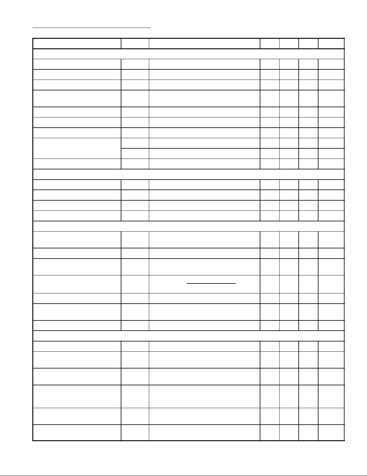
Electrical Characteristics (Cont’d): (TA = +25°C, VCC = V11 = V14 = 9V, ICC = I30 = 13mA unless
otherwise specified)
Parameter Symbol Test Conditions Min Typ Max Unit
VIF (Cont’d)
Maximum AFT Output Voltage V
Minimum AFT Output Voltage V
AFT Detection Sensibility S
AFT Switch Operation Start
V
AFTSW
47H
47L
CW = 80dBµ, frequency change 8.3 8.7 9.0 V
CW = 80dBµ, frequency change 0.1 0.3 0.8 V
CW = 80dBµ, frequency change 45 70 100 mV/kHz
f
Measuring with sweep signal 0.5 1.0 1.5 V
Voltage
Black Noise Threshold Level V
APC Pull–In Range (U)2 f
APC Pull–In Range (L)2 f
PU–2
PL–2
VCO Maximum Variable Range ∆f
∆f
BTH
Measuring with sweep signal 1.1 1.4 1.7 V
CW = 80dBµ, fP = 53MHz to 64MHz 0.8 1.7 4.0 MHz
CW = 80dBµ, fP = 53MHz to 64MHz – –2 –1 MHz
Quiescent 0.9 1.7 4.0 MHz
U
Quiescent –4 –2 –1 MHz
L
VCO Control Sensitivity β Quiescent 1.5 3.0 5.5 kHz/mV
Audio–Visual Switches
Video Output DC Voltage V
Internal Video Input Voltage V
External Video Input Voltage V
External Audio Input Voltage V
Quiescent 3.0 3.4 3.8 V
38
Quiescent 4.4 4.8 5.2 V
42
Quiescent 4.4 4.8 5.2 V
40
Quiescent 5.2 5.6 6.0 V
3
SIF AF
SIF Limiting Voltage Vilim SIF output level for detection output
33 40 47 dBµ
at –3dB
FM Detection Output Voltage VO1 Vi = 100dBµ, ∆f = ±25kHz 440 550 670 mV
FM Detection Output Distortion
THD Vi = 100dBµ, ∆f = ±25kHz 0 0.4 1.0 %
Ratio
FM: ∆f = ±25kHz
AM: 30%
, f = 400Hz 18 20 22 dB
rms
40 60 80 dB
2.0 2.8 3.6 V
AF
Vi = 80dBµ,
Vi = 100mV
AM Rejection AMR
AF Amplifier Voltage Gain G
AF Maximum Output Voltage Vo6 max Output level for AF amplifier output
distortion at 10%
AF Electronic Attenuator Range ATT Vi = 200mV
, f = 400Hz 70 80 100 dB
rms
Video
Black Enhancement Threshold B
Maximum Black Enhancement
BSmax APL variable –35 –27 –20 IRE
STH
APL variable 40 50 60 IRE
Gain
Soft Video Tone Variable Range ∆Soft f = 2MHz, 100mV
P–P
,
–6 –4 –2 dB
video tone VR: 4V → 0V
Sharp Video Tone Variable
Range
∆Sharp f = 2MHz, 100mV
video tone VR: 4V → 9V,
P–P
,
7 10 13 dB
contrast VR: 6V
Video Voltage Gain Audio–Visual
Switch 9V
GV9V f = 100MHz, 100mV
contrast VR: 9V, video, tone VR: 4V
P–P
15 18 21 dB
rms
rms
Video Voltage Gain Audio–Visual
Switch 0V
GV0V f = 100MHz, 100mV
contrast VR: 0V, video tone VR: 4V
P–P
,
15 18 21 dB
 Loading...