

NTE NTE7147 Datasheet

NTE7147
Integrated Circuit
Full Bridge Current Driven Vertical Deflection Booster
Description:
The NTE7147 is a power amplifier in a 9–Lead SIP type package designed for use in 90 degree color
vertical deflection systems for frame frequencies of 50Hz to 160Hz. This device provides a high
CMRR current driven differential input. Due to the bridge configuration of the two output stages, DC–
coupling of the deflection coil is achieved.
Features:
D Pre–Amplifier with Differential High CMRR Current Mode Inputs
D Low Offsets
D High Linear Sawtooth Signal Amplification
D High Efficient DC–Coupled Vertical Output Bridge Circuit
D Powerless Vertical Shift
D High Deflection Frequency up to 160Hz
D Power Supply and Flyback Supply Voltage Independent Adjustable to Optimize Power
Consumption and Flyback Time
D Excellent Transition Behaviour Duriing Flyback
D Guard Circuit for Screen Protection
Absolute Maximum Ratings: (Voltage referenced to Pin5 (GND) unless otherwise specified)
Supply Voltage (Pin3), V
Flyback Supply Voltage (Pin7), V
Flyback Supply Current, I
Input Voltage, V1, V
Input Current, I1, I
2
Output Voltage, V4, V
Output Current (Note 1), I4, I
Feedback Voltage, V
Feedback Current, I
Guard Voltage (Note 2), V
Guard Current, I
8
Operating Junction Temperature Range (Note 3), T
Ambient Temperature Range, T
Storage Temperature Range, T
Thermal Resistance, Junction–to–Mounting Base, R
Electrostatic Handling Voltage (Note 4), V
P
FB
FB
2
±1.8A. . . . . . . . . . . . . . . . . . . . . . . . . . . . . . . . . . . . . . . . . . . . . . . . . . . . . . .
0 to VP V. . . . . . . . . . . . . . . . . . . . . . . . . . . . . . . . . . . . . . . . . . . . . . . . . . . . . . . . . . .
0 to ±5mA. . . . . . . . . . . . . . . . . . . . . . . . . . . . . . . . . . . . . . . . . . . . . . . . . . . . . . . . . . .
6
6
9
9
8
0 to VP V. . . . . . . . . . . . . . . . . . . . . . . . . . . . . . . . . . . . . . . . . . . . . . . . . . . . . . . . .
0 to ±1.8A. . . . . . . . . . . . . . . . . . . . . . . . . . . . . . . . . . . . . . . . . . . . . . . . . .
0 to VP V. . . . . . . . . . . . . . . . . . . . . . . . . . . . . . . . . . . . . . . . . . . . . . . . . . . . . . . . . .
0 to ±5mA. . . . . . . . . . . . . . . . . . . . . . . . . . . . . . . . . . . . . . . . . . . . . . . . . . . . . . . . .
0 to VP+0.4V. . . . . . . . . . . . . . . . . . . . . . . . . . . . . . . . . . . . . . . . . . . . . . . . . .
0 to ±5mA. . . . . . . . . . . . . . . . . . . . . . . . . . . . . . . . . . . . . . . . . . . . . . . . . . . . . . . . . . . . .
J
A
stg
thJ–MB
es
–20° to +150°C. . . . . . . . . . . . . . . . . . . . . . . . . .
–20° to +75°C. . . . . . . . . . . . . . . . . . . . . . . . . . . . . . . . . . . . . . . . . . . .
–20° to +150°C. . . . . . . . . . . . . . . . . . . . . . . . . . . . . . . . . . . . . . . . . .
–500V to +500V. . . . . . . . . . . . . . . . . . . . . . . . . . . . . . . .
Note 1. Maximum output currents I4 and I6 are limited by current protection.
Note 2. For VP > 13V, the guard voltage V8 is limited to 13V.
Note 3. Internally limited by thermal protection; switching point ≥ +150°C.
Note 4. Equivalent to discharging a 200pF capacitor through a 0Ω series resistor,
30V. . . . . . . . . . . . . . . . . . . . . . . . . . . . . . . . . . . . . . . . . . . . . . . . . . . . . . . . . . .
60V. . . . . . . . . . . . . . . . . . . . . . . . . . . . . . . . . . . . . . . . . . . . . . . . . . .
4K/W. . . . . . . . . . . . . . . . . . . . . . . . . . . . .
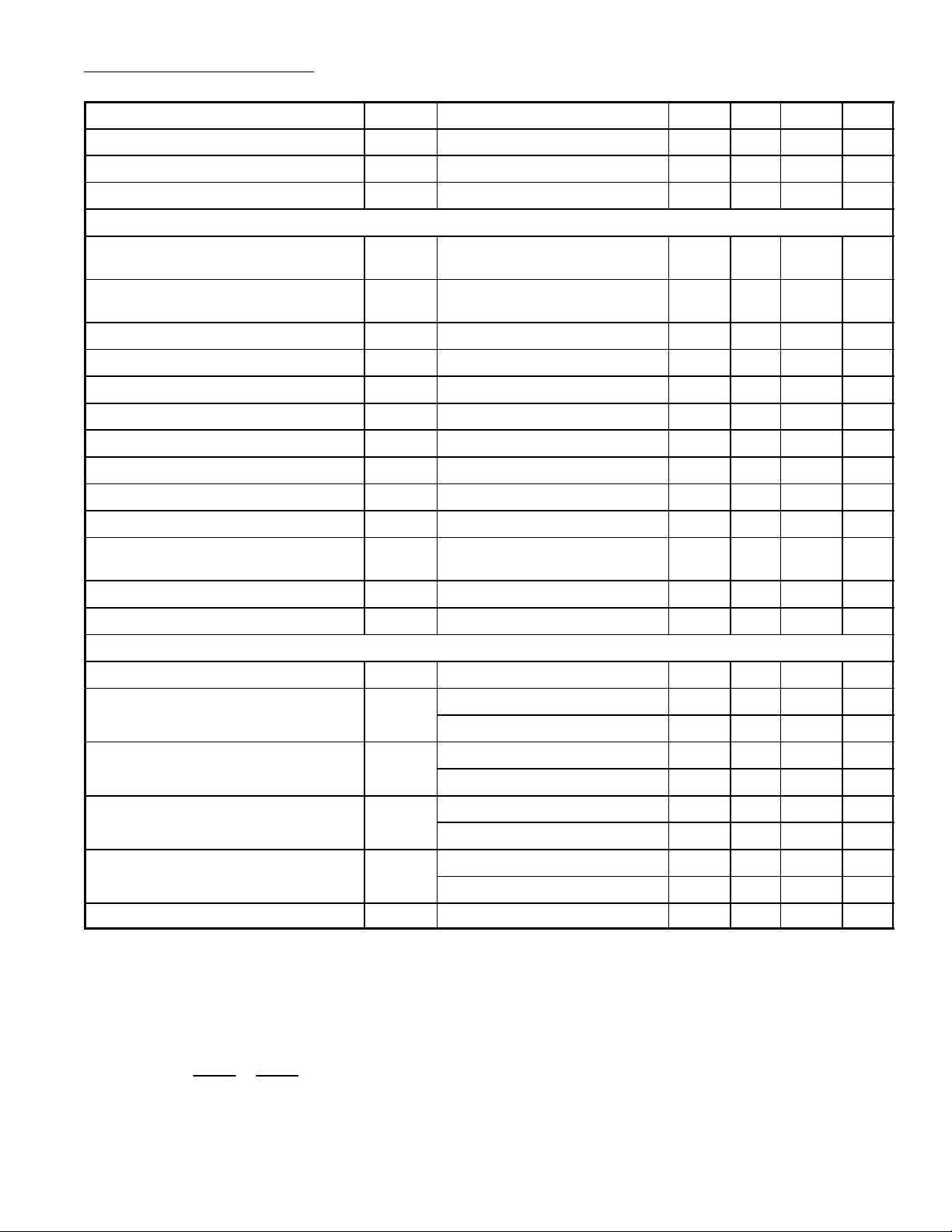
Electrical Characteristics: (VP = 15V, TA = +25°C, VFB = 40V, voltage referenced to Pin5 (GND)
unless otherwise specified)
Parameter Symbol Test Conditions Min Typ Max Unit
Supply Voltage (Pin3) V
Flyback Supply Voltage (Pin7) V
Quiescent Feedback Current (Pin7) I
FB
P
Note 5 VP+6 – 60 V
FB
No Load, No Signal – 7 10 mA
8.2 – 25 V
Input Stage
Differential Input Current (Iid = I1 – I2)
I
id(p–p)
– ±500 ±600 µA
(Peak–to–Peak Value)
Single Ended Input Current
I
1,2(p–p)
Note 6 0 ±300 ±600 µA
(Peak–to–Peak Value)
Common Mode Rejection Ratio CMRR Note 7 – –54 – dB
Input Clamp Voltage V
Input Clamp Signal TC on Pin1 TC
Input Clamp Signal TC on Pin2 TC
Differential Input Voltage V
1
Feedback Current I
Feedback Voltage V
Differential Input Offset Current
(I
id(offset)
= I1 – I2)
I
id(offset)Idefl
Input Capacity Pin1 Reference to GND C
Input Capacity Pin2 Reference to GND C
V
– V
i INA
i INB
I1 = 300µA 2.7 3.0 3.3 V
1
I2 = 300µA 2.7 3.0 3.3 V
2
i,1
i,2
9
9
= 0 0 – ±10 mV
2Iid
= 0, R
= 1.5kΩ, Rm = 1Ω 0 – ±20 µA
ref
0 – ±800 µV/K
0 – ±800 µV/K
– ±500 ±600 µA
1 – VP–1 V
– – 5 pF
– – 5 pF
Output Stages A and B
Output Current I4, I
Output A Saturation Voltage to GND V
6
I6 = 0.7A – 1.3 1.5 V
6
– – ±1 A
I6 = 1.0A – 1.6 1.8 V
Output A Saturation Voltage to V
P
V
I6 = 0.7A – 2.3 2.9 V
6,3
I6 = 1.0A – 2.7 3.3 V
Output B Saturation Voltage to GND V
I4 = 0.7A – 1.3 1.5 V
4
I4 = 1.0A – 1.6 1.8 V
Output B Saturation Voltage to V
P
V
I4 = 0.7A – 1.0 1.6 V
4,3
I4 = 1.0A – 1.3 1.9 V
Linearity Error LE I
= ±0.7A, Note 8 – – 2 %
defl
Note 5. Up to 6 0V ≥ VFB ≥ 4 0V a d ecoupling capaci tor CFB = 22µ(between Pin7 and Pin5) and a r esistor
RFB = 100Ω (between Pin7 and VFB) are required.
Note 6. Saturation voltages of output stages A and B can be increased in the event of negative input
Note 7.
currents I
I
deflc
Di = x with I
I
idc
< –500µA.
1,2
I
id
I
defl
= common mode deflection current and I
deflc
= common mode
idc
input current.
Note 8. Deviation of the output slope at a constant input slope.
 Loading...