

NTE NTE7145 Datasheet

NTE7145
Intergrated Circuit
18W BTL x 2 Ch Audio Power Amplifier
Description:
The NTE7145 is a stereo audio power IC in a 17–Lead Staggered SIP type package designed for car
audio use. This device has 2 built–in channels to reduce the characteristics difference between L and
R channels. In addition, the functions of stand–by, muting, and a variety of protections circuits are
involved.
Features:
D High Power:
P
(1) = 18W (Typ)/Channel (VCC = 14.4V, f = 1kHz, THD = 10%, RL = 4Ω)
OUT
P
(2) = 15W (Typ)/Channel (VCC = 13.2V, f = 1kHz, THD = 10%, RL = 4Ω)
OUT
D Low Distortion Ratio:
THD = 0.04% (Typ) (VCC = 13.2V, f = 1kHz, P
D Low Noise:
VNO = 0.30mV
(Typ) (VCC = 13.2V, RL = 4Ω, GV = 50dB, Rg = 0Ω, BW = 20Hz to 20kHz)
rms
D Built–In Stand–By Function (With Pin4 set at Low, Power is Turned OFF):
ISB = 1µA (Typ)
D Built–In Muting Function (With Pin1 set at Low, Power is Turned OFF):
V (Mute) = 1V (Typ)
D Built–In Various Protection Circuits:
Thermal Shut Down
Overvoltage
OUT→VCC Short
OUT→GND Short
OUT–OUT Short
D Operating Supply Voltage: VCC = 9V to 18V
= 1W, RL = 4Ω, GV = 50dB)
OUT
Absolute Maximum Ratings: (TA = +25°C unless otherwise specified)
Peak Supply Voltage (0.2s), VCCsurge 50V. . . . . . . . . . . . . . . . . . . . . . . . . . . . . . . . . . . . . . . . . . . . . . . .
DC Supply Voltage, VCCDC 25V. . . . . . . . . . . . . . . . . . . . . . . . . . . . . . . . . . . . . . . . . . . . . . . . . . . . . . . . . .
OPerating Supply Voltage, VCCopr 18V. . . . . . . . . . . . . . . . . . . . . . . . . . . . . . . . . . . . . . . . . . . . . . . . . . .
Output Current (Peak), I
Power Dissipation, P
Operating Temperature Range, T
Storage Temperature Range, T
D
O(peak)
stg
opr
–30° to +85°C. . . . . . . . . . . . . . . . . . . . . . . . . . . . . . . . . . . . . . . . .
–55° to +150°C. . . . . . . . . . . . . . . . . . . . . . . . . . . . . . . . . . . . . . . . . .
9A. . . . . . . . . . . . . . . . . . . . . . . . . . . . . . . . . . . . . . . . . . . . . . . . . . . . . . . .
50W. . . . . . . . . . . . . . . . . . . . . . . . . . . . . . . . . . . . . . . . . . . . . . . . . . . . . . . . . . . . .
Electrical Characteristics: (TA = +25°C, VCC = 13.2V, RL = 4Ω, f = 1kHz, unless otherwise specified)
Parameter Symbol Test Conditions Min Typ Max Unit
Quiescent Supply Current I
Output Power P
CCQ
OUT
Total Harmonic Distortion THD P
Voltage Gain G
Output Noise Voltage V
NO
Ripple Rejection Ratio RR f
Input Resistance R
Output Offset Voltage V
Current at Stand–By State I
offset
SB
Crosstalk CT Rg = 600Ω, V
Pin4 Control Voltage V
Pin1 Control Voltage V
(SB)
(MUTE)
VIN = 0 – 120 250 mA
VCC = 14.4V, THD = 10% – 18 – W
THD = 10% 11 15 – W
= 1W – 0.04 0.4 %
OUT
V
48 50 52 dB
Rg = 0Ω, BW = 20Hz to 20kHz – 0.3 0.7 mV
= 100Hz, Rg = 600Ω 40 54 – dB
ripple
IN
– 30 – kΩ
VIN = 0 –0.3 0 +0.3 V
– 1 10 µA
= 0.775V
OUT
(0dBm) – 60 – dB
rms
Stand–By→OFF (Power→ON) 2.5 – V
Mute→ON (Power→OFF) – 1.0 2.0 V
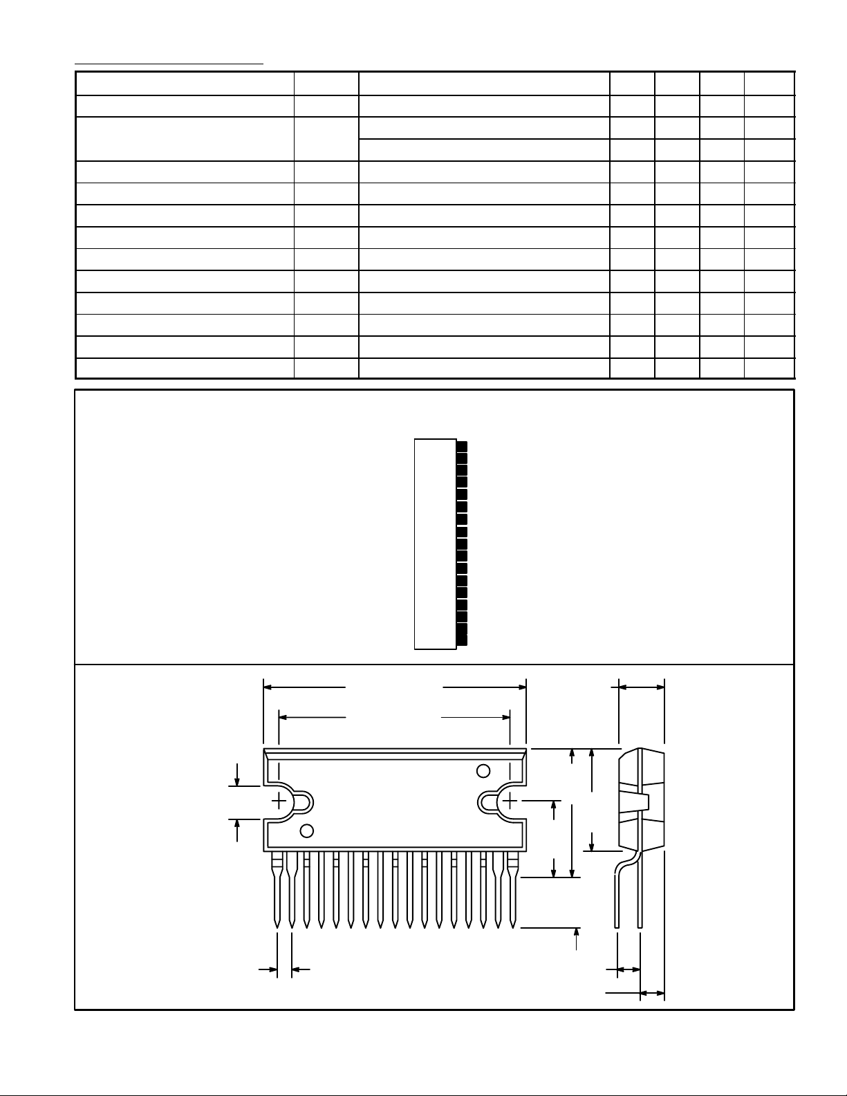
Pin Connection Diagram
(Front View)
Power VCC2
17
Output 216
Output 1
15
GND 1
14
13
GND 2
Output 4
12
Output 3
11
Power VCC1
10
Pre–V
9
CC
Ripple
8
Input 2
7
NF 2
6
Pre–GND
5
Stand–By Switch
4
NF 1
3
Input 1
2
Mute Switch
1
CC
rms
V
.154
(3.9)
1.440 (36.6)
.197 (5.0)
1.180 (30.0)
.670
(17.0)
.550
(14.0)
117
.394
(10.0)
.197
(5.0)
.079 (2.0)
.079 (2.0)
.101 (2.56)
 Loading...