

NTE NTE7142 Datasheet

NTE7142
Integrated Circuit
+5V–Powered, Multichannel RS–232 Driver/Receiver
Description:
The NTE7142 is a multichannel RS–232 driver/receiver in a 16–Lead DIP type package intended for
all EIA/TIA–232E and V.28/V.24 communications interfaces, particularly applications where ±12V is
not available.
Features:
D Operate From Single +5V Power Supply
D Meet All EIA/TIA–232E and V.28 Specifications
D Multiple Drivers and Receivers
D 3–State Driver and Receiver Outputs
Applications:
D Portable Computers
D Low–Power Modems
D Interface Translation
D Battery–Powered RS–232 Systems
D Multidrop RS–232 Networks
Absolute Maximum Ratings: (Note 1)
Supply Voltage, V
Input Voltage, T
Input Voltage, R
CC
IN
IN
Output Voltage (Note 2), T
Output Voltage, R
OUT
–0.3V to (VCC–0.3V). . . . . . . . . . . . . . . . . . . . . . . . . . . . . . . . . . . . . . . . . . . . . . . . . . .
OUT
–0.3V to (VCC+0.3V). . . . . . . . . . . . . . . . . . . . . . . . . . . . . . . . . . . . . . . . . . . . . . . .
–0.3V to +6V. . . . . . . . . . . . . . . . . . . . . . . . . . . . . . . . . . . . . . . . . . . . . . . . . . . . . . . .
±30V. . . . . . . . . . . . . . . . . . . . . . . . . . . . . . . . . . . . . . . . . . . . . . . . . . . . . . . . . . . . . . . . .
±15V. . . . . . . . . . . . . . . . . . . . . . . . . . . . . . . . . . . . . . . . . . . . . . . . . . . . . .
Driver/Receiver Output Short Circuited to GND Continuous. . . . . . . . . . . . . . . . . . . . . . . . . . . . . . . . . .
Continuous Power Dissipation (TA = +70°C), P
D
842mW. . . . . . . . . . . . . . . . . . . . . . . . . . . . . . . . . . . . .
Dreate Above +70°C 10.53mW/°C. . . . . . . . . . . . . . . . . . . . . . . . . . . . . . . . . . . . . . . . . . . . . . . . . .
Operating Temperature Range, T
Storage Temperature Range, T
opr
stg
Lead Temperature (During Soldering, 10sec), T
L
0° to +70°C. . . . . . . . . . . . . . . . . . . . . . . . . . . . . . . . . . . . . . . . . . .
–65° to +160°C. . . . . . . . . . . . . . . . . . . . . . . . . . . . . . . . . . . . . . . . . .
+300°C. . . . . . . . . . . . . . . . . . . . . . . . . . . . . . . . . . . .
Note 1. Stresses beyond those listed under “Absolute Maximum Ratings” may cause permanent
damage to the device. These are stress ratings only, and functional operation of the device
at these or any other conditions beyond those indicated in the operational section of the
specifications is not implied. Exposure to absolute maximum rating conditions for extended
periods may affect device reliability.
Note 2. Input voltage measured with T
in high–impedance state, VCC = 0V.
OUT
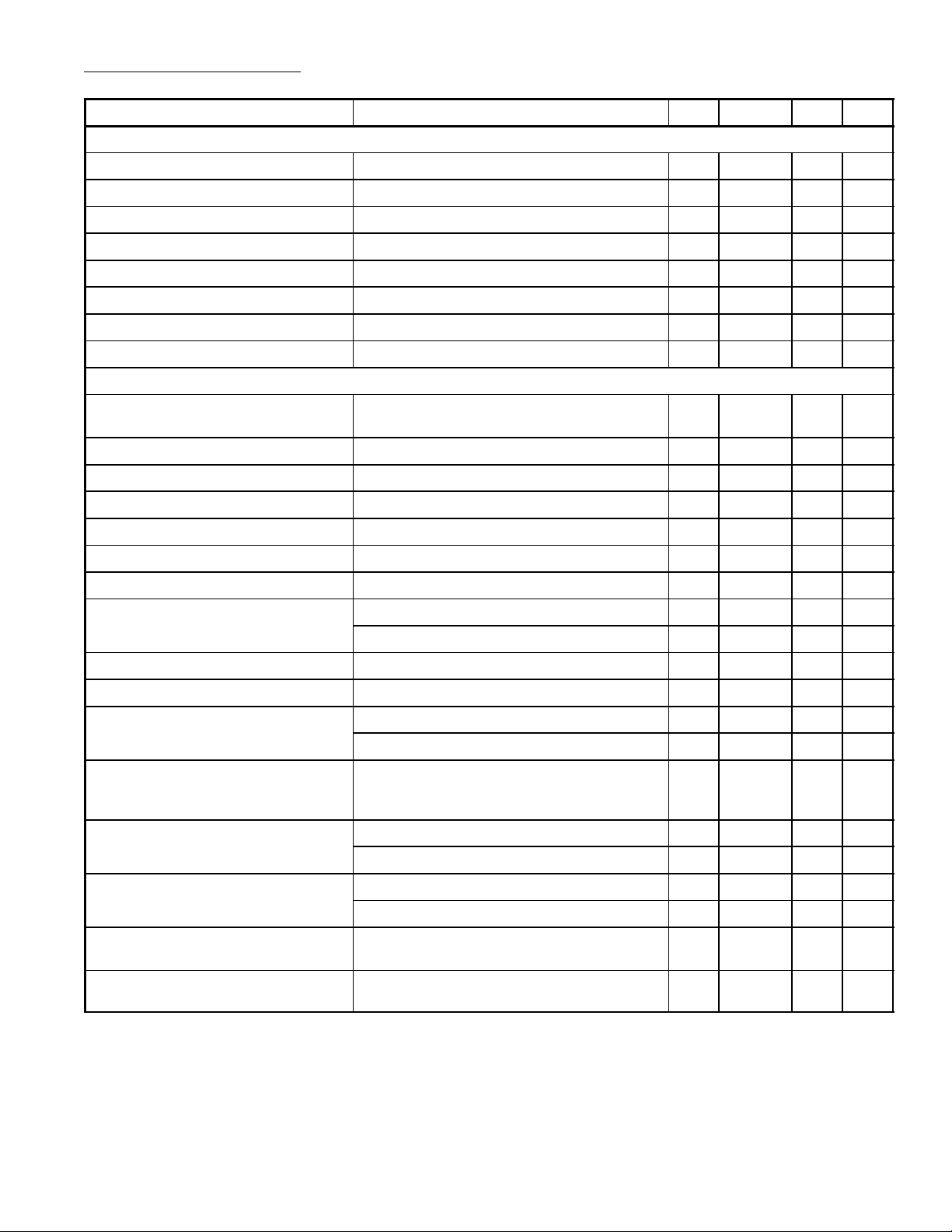
Electrical Characteristics: (VCC = +5 V ±10%, TA = 0° to +70°C, C1–C4 = 0.1µF unless otherwise
specified)
Parameter Test Conditions Min Typ Max Unit
RS–232 Transmitter
Output Voltage Swing All transmitter output loaded with 3kΩ to GND ±5 ±8 – V
Input Logic Threshold Low – 1.4 0.85 V
Input Logic Threshold High 2.0 1.4 – V
Logic Pull–Up/Input Current Normal operation – 5 40 µA
Output Leakage Current VCC = 0V, V
= ±15V – ±0.01 ±10 µA
OUT
Data Rate Normal operation – 200 116 kb/s
Transmitter Output Resistance VCC = V+ = V– = 0V, V
Output Short–Circuit Current V
= 0V ±7 ±22 – mA
OUT
= ±2V 300 10M – Ω
OUT
RS–232 Receiver
RS–232 Input Voltage Operating
– – ±30 V
Range
RS–232 Input Threshold Low VCC = 5V, R2
RS–232 Input Threshold High VCC = 5V, R2
IN
IN
0.8 1.3 – V
– 1.8 2.4 V
RS–232 Input Hysteresis VCC = 5V 0.2 0.5 1.0 V
RS–232 Input Resistance 3 5 7 kΩ
TTL/CMOS Output Voltage Low I
TTL/CMOS Output Voltage High I
TTL/CMOS Output Short–Circuit
Current
TTL/CMOS Output Leakage Current 0V ≤ V
= 3.2mA – 0.2 0.4 V
OUT
= –1.0mA 3.5 VCC–0.2 – V
OUT
Sourcing, V
Shrinking, V
OUT
= GND –2 –10 – mA
OUT
OUT
≤ V
CC
= V
CC
10 30 – mA
– ±0.05 ±10 µA
Operating Supply Voltage 4.5 – 5.5 V
VCC Supply Current No load – 4 10 mA
3kΩ load, both inputs – 15 – mA
Transition Slew Rate CL = 50pF to 2500pF, RL = 3kΩ to 7kΩ,
VCC = 5V, TA = +25°C, measured from
+3V to –3V or –3V to +3V
Transmitter Propagation Delay
TTL to RS–232 (normal operation)
Receiver Propagation Delay
RS–232 to TTL (normal operation)
Transmitter + to – Propagation Delay
t
PHLT
t
PLHT
t
PHLR
t
PLHR
t
PHLT
– t
PLHT
Difference (normal operation)
Receiver + to – Propagation Delay
t
PHLR
– t
PLHR
Difference (normal operation)
6 12 30 V/µs
– 1.3 3.5 µs
– 1.5 3.5 µs
– 0.5 1.0 µs
– 0.6 1.0 µs
– 300 – ns
– 100 – ns
 Loading...