

NTE NTE714 Datasheet
NTE714
Integrated Circuit
Chroma Subcarrier Regeneration
Features:
D DC Hue Control
D Phase Locked Oscillator
D Keyed APC and ACC Detector
D Internal Shunt Voltage Regulator
D 16–Pin Dual In–Line Plastic Package
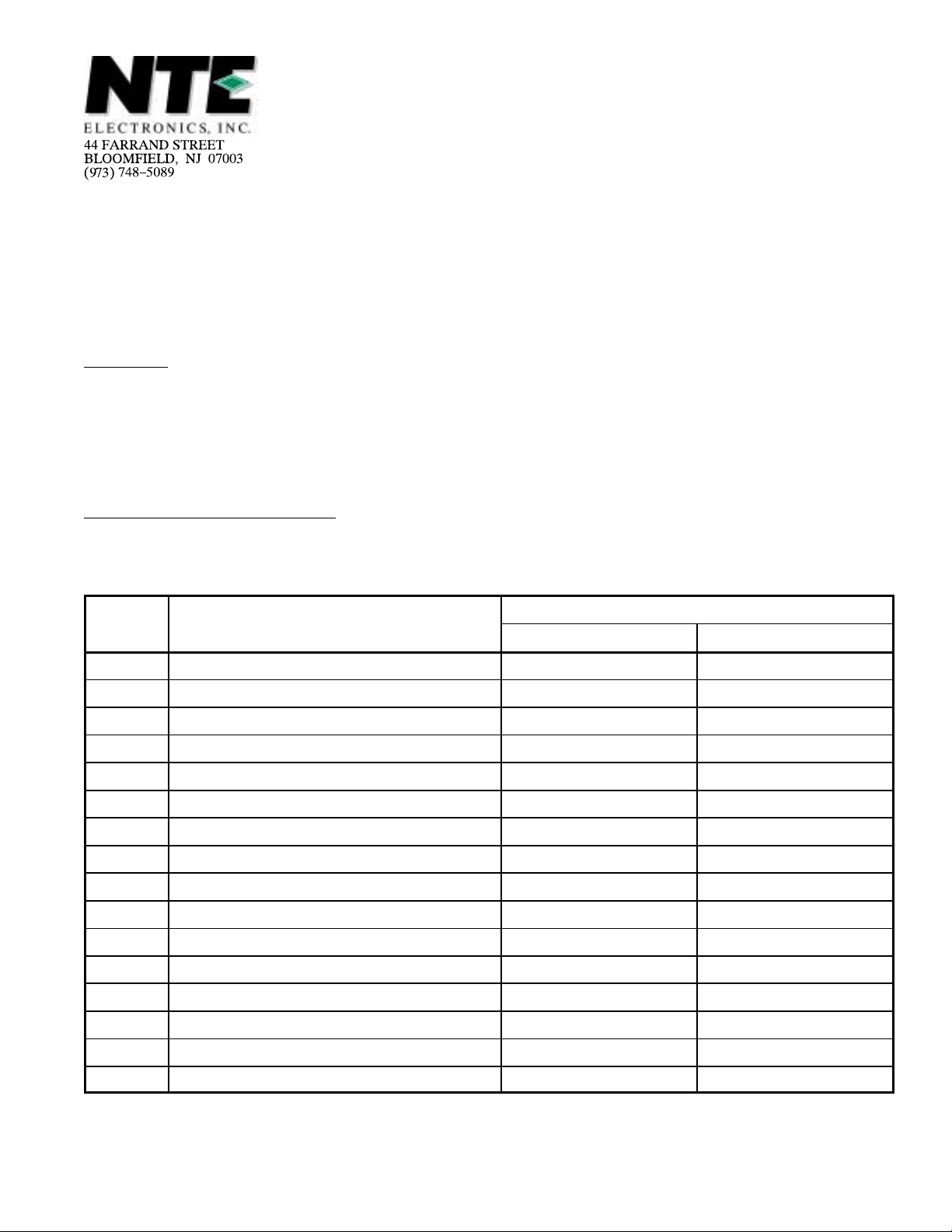
Absolute Maximum Ratings:
Operating Temperature Range, TA –40°C to +85°C. . . . . . . . . . . . . . . . . . . . . . . . . . . . . . . . . . . . . . . .
Storage Temperature Range, Ts –65°C to +150°C. . . . . . . . . . . . . . . . . . . . . . . . . . . . . . . . . . . . . . . . .
Maximum Voltage and Current Ratings (TA = +25°C) See Table. . . . . . . . . . . . . . . . . . . . . . . . . . . . . .
Current in mA
Pin # Voltage Range in Volts
Input Output
1 0 to +10 20 1.0
2 0 to +16 – –
3 0 to +16 – –
4 6.0 to 0 (Note 1) 20 1.0
5 reference 1.0 50
6 0 to +5.0 – –
7 0 to V
8 0 to V
REG
REG
– –
– –
9 No Connection – –
10 Note 2 50 1.0
11 0 to V
12 0 to V
13 0 to V
14 0 to V
REG
REG
REG
REG
– –
– –
20 1.0
20 1.0
15 0 to +16 – –
16 0 to –16 – –
Note 1. Limited by input current
Note 2. Dependent on value of external current limiting resistor, 0 to 11V at 0Ω
Static Electrical Characteristics: (TA = +25°C unless otherwise specified)
Parameter Test Pins Test Conditions Min Typ Max Unit
Static Characteristics
Regulator Voltage 10 ICC = 25mA 11.3 – 12.9 V
Oscillator Current 2 to 3 Sw1: Low; Sw2: High 4.1 – 7.6 mA
ACC Leakage 15 to 16 Sw1: High; Sw2: Low, Ref Pin10 – 5 30 mV
APC Leakage 11 to 12 Sw1: High; Sw2: Low, Ref Pin10 – 40 80 mV
ACC Balance 15 to 16 Sw1: High; Sw2: High, Pin16 = –DVM –330 – +300 mV
APC Balance 11 to 12 Sw1: High; Sw2: High, Pin12 = –DVM –375 – +375 mV
Oscillator Balance 7 to 8 Sw1: High; Sw2: Low, Pin8 = –DVM –330 – +330 mV
Dynamic Characteristics
Frequency Pull–In Range 11 to 12 Burst = 0.4V
Subcarrier Output Level and
Hue Control
3 to 2 R1: High, Pin2 = DVM +350 – – mV
R1: Low, Pin2 = DVM –350 – – mV
ACC Output Level 15 to 16 Burst = 0.4V
Free Running Oscillator
2 or 3 Snort Pin11 to Pin12 3.579
Frequency
, Note 1 +200 – – Hz
P–P
, Note 2 120 150 – mV
P–P
– 3.579
245
845
Note 1. Limited by input current
Note 2. Dependent on value of external current limiting resistor, 0 to 11V at 0Ω
MHz
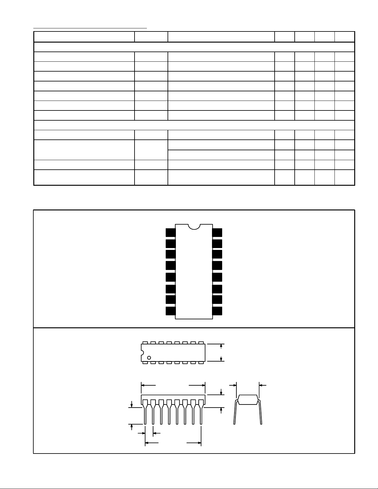
Pin Connection Diagram
Tint Control
OSC Output
OSC Output
Gate In
16 9
18
.785 (19.9)
.245
(6.22)
Min
1
2
3
4
5GND
6OSC Feedback
7OSC Control
8OSC Control
Max
ACC Det Output
16
ACC Det Output
15
ACC Det Input
14
APC Det Input
13
12 APC Det Output
11 APC Det Output
10
V
CC
N.C.
9
.260 (6.6) Max
.300
(7.62)
.200 (5.08)
Max
.100 (2.54)
.700 (17.7)
 Loading...