

NTE NTE7134 Datasheet

NTE7134
Integrated Circuit
Horizontal and Vertical Deflection Controller
for Monitors
Description:
The NTE7134 is a high performance and efficient solution for autosync monitors in a 32–Lead DIP
type package. The concept is fully DC controllable and can be used in applications with a microcontroller and stand–alone in rock bottom solutions.
This device provides synchronization processing, H + V synchronization with full autosync capability ,
and very short setting times after mode changes. External power components are givena great deal
of protection. The IC generates the drive waveforms for DC–coupled vertical boosters.
The NTE7134 provides ectended functions e.g. as a flexible SMPS block and an extensive set of geometry control facilities, providing excellent picture quality.
Features:
Concept Features
D Full Horizontal (H) Plus Vertical (V) Autosync Capability
D Completely DC Controllable for Analog and Digital Concepts
D Excellent Geometry Control Functions (e.g. Automatic Correction of East–West (EW) Parabola
During Adjustment of Vertical Size and Vertical Shift)
D Felxible Switched Mode Power Supply (SMPS) Function Block for Feedback and Feed Forward
Converters.
D X–Ray Protection
D Start–Up and Switch–Off Sequences for safe Operation of All Power Components
D Very Good Vertical Linearity
D Internal Supply Voltage Stabilization
Synchronization Inputs
D Can Handle All Sync Signals (Horizontal, Vertical, Composite and Sync–On–Video)
D Combined Output for Video Clamping, Vertical Blanking and Protection Blanking
D Start of Video Clamping Pulses Externally Selectable
Horizontal Section
D Extremely Low Jitter
D Frequency Locked Loop for Smooth Catching of Line Frequrncy
D Simple Frequency Preset of f
D DC Controllable Wdie Range Linear Picture Position
D Soft Start for Horizontal Driver
Vertical Section
D Vertical Amplitude Independent of Frequency
D DC Controllable Picture Height, Picture Position and S–Correction
D Differential Current Outputs for DC Coupling to Vertical Booster
min
and f
by External Resistors
max
Features (Cont’d):
EW Section
D Output for DC Adjustable EW Parabola
D DC Controllable Picture Width and Trapezium Correction
D Optional Tracking of EW Parabola with Line Frequency
D Prepared for Additional DC Controls of Vertical Linearity, EW–Corner, EW Pin Balance, EW
Parallelogram, Vertical Focus by Extended Application
Absolute Maximum Ratings: (All voltages measured with respect to GND)
Supply Voltage (Pin9), V
Input Voltages, V
I(n)
CC
–0.5 to +16V. . . . . . . . . . . . . . . . . . . . . . . . . . . . . . . . . . . . . . . . . . . . . . . . . .
Pin5 –0.5 to +6.0V. . . . . . . . . . . . . . . . . . . . . . . . . . . . . . . . . . . . . . . . . . . . . . . . . . . . . . . . . . . . . . .
Pin15, Pin17, Pin18, Pin19, Pin23, Pin28, Pin30 –0.5 to +6.5V. . . . . . . . . . . . . . . . . . . . . . . .
Pin2 –0.5 to +8.0V. . . . . . . . . . . . . . . . . . . . . . . . . . . . . . . . . . . . . . . . . . . . . . . . . . . . . . . . . . . . . . .
Pin10 –0.5 to +16V. . . . . . . . . . . . . . . . . . . . . . . . . . . . . . . . . . . . . . . . . . . . . . . . . . . . . . . . . . . . . . .
Output Voltages, V
O(n)
Pin12, Pin13 –0.5 to +6.5V. . . . . . . . . . . . . . . . . . . . . . . . . . . . . . . . . . . . . . . . . . . . . . . . . . . . . . . .
Pin6, Pin7 –0.5 to +16V. . . . . . . . . . . . . . . . . . . . . . . . . . . . . . . . . . . . . . . . . . . . . . . . . . . . . . . . . . .
Input/Output Voltages, V
IO(n)
Pin3, Pin4 –0.5 to +6.0V. . . . . . . . . . . . . . . . . . . . . . . . . . . . . . . . . . . . . . . . . . . . . . . . . . . . . . . . . .
Pin14 –0.5 to +6.5V. . . . . . . . . . . . . . . . . . . . . . . . . . . . . . . . . . . . . . . . . . . . . . . . . . . . . . . . . . . . . .
Horizontal Driver Output Current, I
Horizontal Flyback Input Current, I
HDRV
HFLB
Video Clamping Pulse/Vertical Blanking Output Current, I
B+ Control OTA Output Current, I
B+ Control Driver Output Current, I
EW Driver Output Current, I
Electrostatic Discharge for All Pins (Note 1), V
BOP
BDRV
EWDRV
esd
CLBL
–10 to +10mA. . . . . . . . . . . . . . . . . . . . . . . . . . . . . . . . . . . . . .
100mA. . . . . . . . . . . . . . . . . . . . . . . . . . . . . . . . . . . . . . . . . . . . .
–10mA. . . . . . . . . . . . . . . . . . . . . . . .
50mA. . . . . . . . . . . . . . . . . . . . . . . . . . . . . . . . . . . . . . . . . . . . .
–5mA. . . . . . . . . . . . . . . . . . . . . . . . . . . . . . . . . . . . . . . . . . . . . . . . . .
Machine Model ±400V. . . . . . . . . . . . . . . . . . . . . . . . . . . . . . . . . . . . . . . . . . . . . . . . . . . . . . . . . . . .
Human Body Model ±3000V. . . . . . . . . . . . . . . . . . . . . . . . . . . . . . . . . . . . . . . . . . . . . . . . . . . . . . .
Operating Junction Temperature, T
Operating Ambient Temperatrure Range, T
Storage Temperature Range, T
J
A
stg
Thermal Resistance, Junction–to–Ambient (In Free Air), R
–55° to +150°C. . . . . . . . . . . . . . . . . . . . . . . . . . . . . . . . . . . . . . . . . .
thJA
+150°C. . . . . . . . . . . . . . . . . . . . . . . . . . . . . . . . . . . . . . . . . . . . . . .
0° to +70°C. . . . . . . . . . . . . . . . . . . . . . . . . . . . . . . . . . . .
55K/W. . . . . . . . . . . . . . . . . . . . . . . .
1mA. . . . . . . . . . . . . . . . . . . . . . . . . . . . . . . . . . . . . . . . . . . . . . . .
Note 1. Machine model: 200pF, 25Ω, 2.5µH; Human body model: 100pF, 1500Ω, 7.5µH.
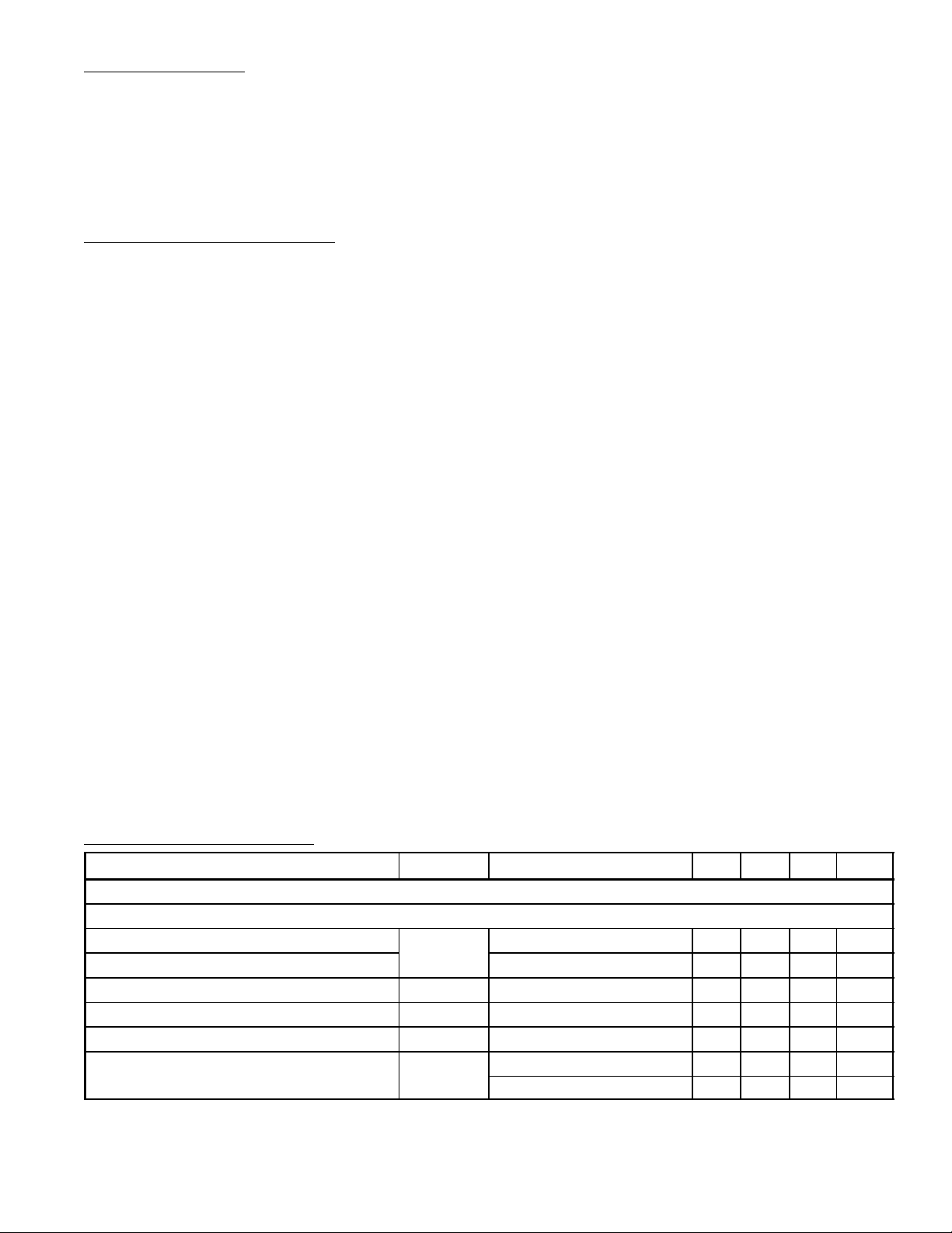
Electrical Characteristics: (VP = 12V, TA = +25°C unless otherwise specified)
Parameter Symbol Test Conditions Min Typ Max Unit
Horizontal Sync Separator
Input Characteristics for DC–Coupled TTL Signals [HSYNC (Pin15)]
Sync Input Signal Voltage V
Slicing Voltage Level 1.2 1.4 1.6 V
Rise Time of Sync Pulse t
Fall Time of Sync Pulse t
Minimum Width of Sync Pulse t
Input Current I
DC(HSYNC)
r(HSYNC)
f(HSYNC)
W(HSYNC)
DC(HSYNC)VHSYNC
V
HSYNC
= 0.8V – – –200 µA
= 5.5V µA
1.7 – – V
10 – 500 ns
10 – 500 ns
0.7 – – µs
Electrical Characteristics (Cont’d): (VP = 12V, TA = +25°C unless otherwise specified)
Parameter Symbol Test Conditions Min Typ Max Unit
Horizontal Sync Separator (Cont’d)
Input Characteristics for AC–Coupled Video Signals (Sync–on–Video, Negative Sync Polarity)
Sync Amplitude of Video Input Signal
Voltage
Slicing Voltage Level
(Measured from Top Sync)
Top Sync Clamping Level V
Charge Current for Coupling Capacitor I
Minimum Width of Sync Pulse t
Maximum Source Resistance R
Differential Input Resistance r
Automatic Polarity Correction for Horizontal Sync
Horizontal Sync Pulse Width Related to t
Delay Time for Changing Polarity t
Vertical Sync Integrator
Integration Time for Generation of a
Vertical Trigger Pulse
Vertical Sync Slicer (DC–Coupled, TTL Compatible) [VSYNC (Pin14)]
Sync Input Signal Voltage V
Slicing Voltage Level 1.2 1.4 1.6 V
Input Current I
Vertical Sync Output at VSYNC (Pin14) During Composite Sync at HSYNC (Pin15)
Output Current I
Internal Clamping Voltage Level V
Steepness of Slopes – 300 – ns/mA
Automatic Polarity Correction for Vertical Sync
Maximum Width of Vertical Sync Pulse t
Delay for Change Polarity t
Video Clamping/Vertical Blanking Output [CLCB (Pin16)]
Width of Video Clamping Pulse t
Temperature Coefficient of V
clamp(CLCB)
Steepness of Slopes for Clamping Pulse RL = 1MΩ, CL = 20pF – 50 – ns/V
Top Voltage Level of Vertical
Blanking Pulse
Width of Vertical Blanking Pulse t
H
V
AC(HSYNC)
clamp(HSYNC)
C(HSYNC)
HSYNC(min)
S(max)
diff(HSYNC)
t
p(H)
t
H
p(H)
t
int(V)
VSYNC
VSYNC
VSYNC
VSYNC
VSYNC(max)
d(VPOL)
clamp(CLBL)
TC
clamp
V
blank(CLBL)
blank(CLBL)
– 300 – mV
RS = 50Ω 90 120 150 mV
1.1 1.28 1.5 V
V
HSYNC
> V
clamp(HSYNC)
1.7 2.4 3.4 µA
0.7 – – µs
Duty factor = 7% – – 1500 Ω
During Sync – 80 – Ω
fH < 45kHz – – 20 %
fH > 45kHz – – 25 &
0.3 – 1.8 ms
fH = 31.45kHz,
I
= 1.052mA
HREF
fH = 64kHz,
I
= 2.141mA
HREF
fH = 100kHz,
I
= 3.345mA
HREF
7.0 10.0 13.0 µs
3.9 5.7 6.5 µs
2.5 3.8 4.5 µs
1.7 – – V
0V < V
< 5.5V – – ±10 µA
SYNC
During Internal Vertical Sync –0.7 –1.0 –1.35 mA
During Internal Vertical Sync 4.4 4.8 5.2 V
– – 300 µs
0.3 – 1.8 ms
Measured at V
= 3V 0.6 0.7 0.8 µs
CLBL
– +4 – mV/K
Note 2 1.7 1.9 2.1 V
240 300 360 µs
Note 2. Continuous blanking at CLCB (Pin16) will be activated, if one of the following conditions is true:
a) No horizontal flyback pulse at HFLB (Pin1) within a line
b) X–ray protection is triggered
c) Voltage at HPLL2 (Pin31) is low (for soft start of horizontal drive)
d) Supply voltage at VVV (Pin9) is low
e) PLL1 unlocked while frequency–locked loop is in search mode
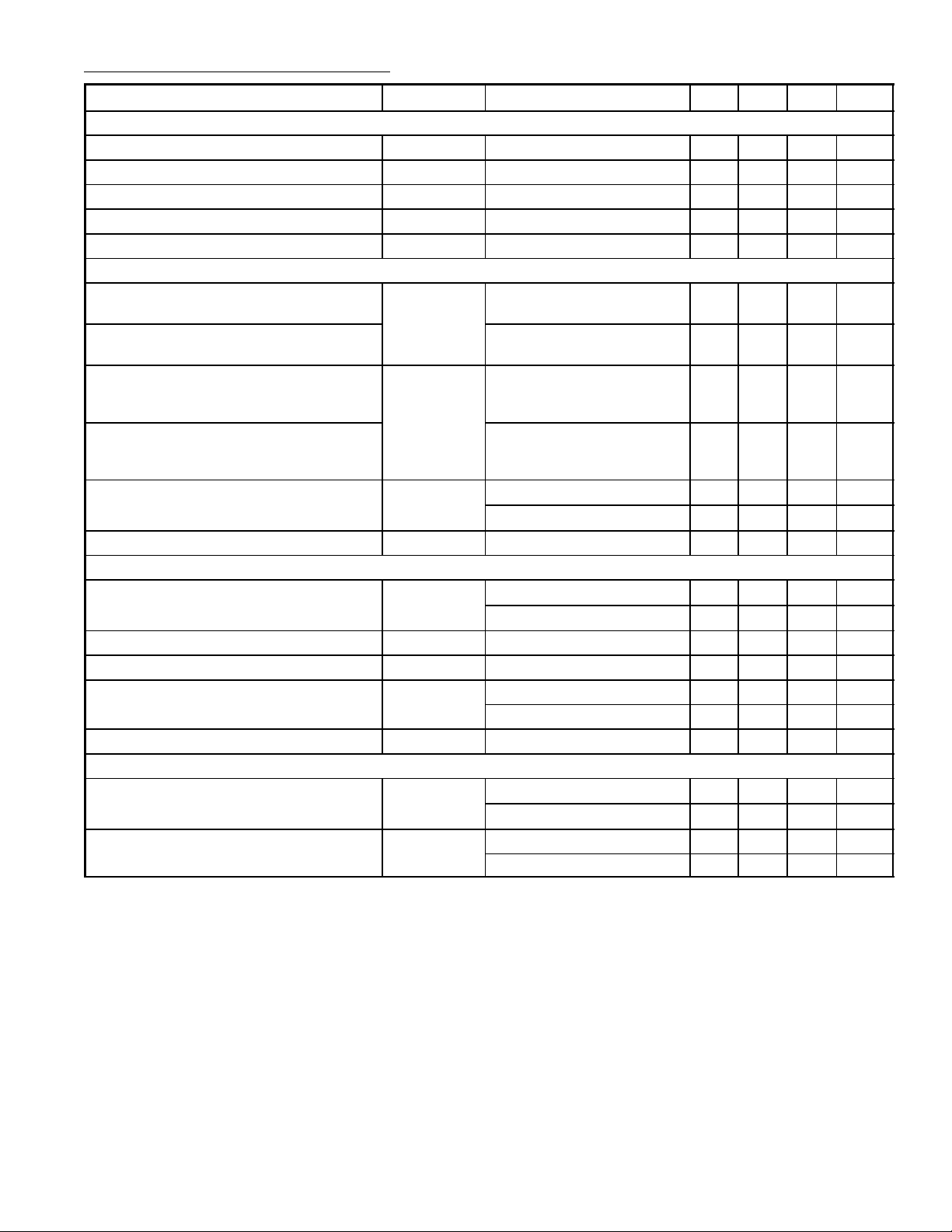
Electrical Characteristics (Cont’d): (VP = 12V, TA = +25°C unless otherwise specified)
Parameter Symbol Test Conditions Min Typ Max Unit
Video Clamping/Vertical Blanking Output (Cont’d) [CLCB (Pin16)]
Temperature Coefficient of V
blank(CLBL)
Output Voltage During Vertical Scan V
Temperature Coefficient of V
scan(CLBL)
Internal Sink Current I
External Load Current I
Selection of Leading/Trailing Edge for Video Clamping Pulse
Voltage at CLSEL (Pin10) for Trigger with
Leading Edge of Horizontal Sync
Voltage at CLSEL (Pin10) for Trigger with
Trailing Edge of Horizontal Sync
Delay Between Leading Edge of
Horizontal Sync and Start of
Horizontal Clamping Pulse
Delay Between Leading Trailing of
Horizontal Sync and Start of
Horizontal Clamping Pulse
Maximum Duration of Video Clamping
Pulse After End of Horizontal Sync
Input Resistance at CLSEL (Pin10) R
PLL1 Phase Comparator and Frequency–Locked Loop [HPLL1 (Pin26) and HBUF (Pin27)]
Maximum Width of Horizontal Sync Pulse
(Referenced to Line Period)
Total Lock–In Time of PLL1 t
Control Voltage V
Buffered f/v Voltage at HBUF (Pin27) V
Maximum Load Current I
Adjustment of Horizontal Picture Position
Horizontal Shift Adjustment Range
(Referenced to Horizontal Period)
Input Current I
TC
blank
scan(CLBL)ICLBL
TC
scan
sink(CLBL)
load(CLBL)
V
CLSEL
t
d(clamp)
V
V
t
clamp(max)
V
V
CLSEL
t
HSYNC(max)fH
V
fH > 45kHz, Note 3 – – 25 %
lock(HPLL1)
HPLL1
HBUF
Note 4, Note 5
f
f
load(HBUF)
∆HPOS I
I
HPOS
∆HPOS = +10.5% –110 –120 –135 µA
∆H POS = –10.5% – 0 – µA
– +2 – mV/K
= 0 0.59 0.63 0.67 V
– –2 – mV/K
2.4 – – mA
– – –3.0 mA
7 – V
0 – 5 V
> 7V – 300 – ns
CLSEL
< 5V – 130 – ns
CLSEL
CLBL
CLBL
CLSEL
= 3V, V
= 3V, V
≤ V
CC
> 7V – – 0.15 µs
CLSEL
> 5V – – 1.0 µs
CLSEL
80 – – kΩ
< 45kHz, Note 2 – – 20 &
– 40 80 ms
, Note 6 – 5.6 – V
H(min)
, Note 6 – 2.5 – V
H(max)
– – –4.0 mA
= 0 – –10.5 – %
HSHIFT
= –135µA – +10.5 – %
HSHIFT
CC
V
Note 3. To ensure safe locking of the horizontal oscillator , one of the following procedures is required :
a) Search mode starts always from f
. Then the PLL1 filter components are a 3.3nF
min
capacitor from Pin26 to GND in parallel with an 8.2kΩ resistor in series with a 47nF
capacitor.
b) Search mode starts either from f
min
or f
with HPOS in m iddle position (I
max
HPOS
= 60µA).
Then the PLL1 filter components are a 1.5nF capacitor from Pin26 to GND in parallel
with a 27kΩ resistor in series with a 47nF capacitor.
c) After locking is achieved, HPOS can be operated in the normal way
Note 4. Loading of HPLL1 (Pin26) is not allowed.
Note 5. Oscillator frequency is f
when no sync signal is present (no continuous blanking at Pin16).
min
Note 6. V oltage at HPPL1 (Pin26) is fed to HBUF (Pin27) via a buffer. Disturbances caused by hori-
zontal sync are removed by an internal sample–and–hold circuit.
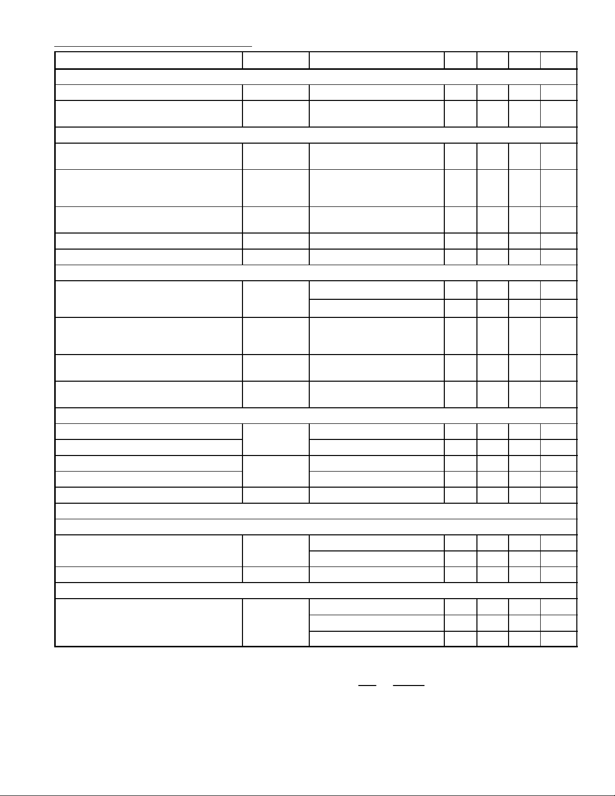
Electrical Characteristics (Cont’d): (VP = 12V, TA = +25°C unless otherwise specified)
Parameter Symbol Test Conditions Min Typ Max Unit
Adjustment of Horizontal Picture Position (Cont’d)
Reference Voltage at Input V
Picture Shift is Centered if
ref(HPOS)
V
off(HPOS)
HPOS (Pin30) is Forced to GND
Horizontal Oscillator [HCAP (Pin29) and HREF (Pin28)]
Free–Running Frequency Without PLL1
f
H(0)
Action (For Testing Only)
Spread of Free–Running Frequency
∆f
H(0)
(Excluding Spread of External
Components)
Temperature Coefficient of
TC –100 – +100 10–6/K
Free–Running Frequency
Maximum Oscillator Frequency f
Voltage at Input for Reference Current V
H(max)
HREF
PLL2 Phase Detector [HFLB (Pin1) and HPPL2 (Pin31)]
PLL2 Control (Advance of Horizontal
∆φ
PLL2
Drive with Respect to Middle of
Horizontal Flyback)
Delay Between Middle of Horizontal
t
d(HFLB)
Sync and Middle of Horizontal
Flyback
Maximum Voltage for PLL2 Protection
V
PROT(HPLL2)
Mode/Soft Start
Charge Current for External Capacitor
I
charge(HPLL2)VHPLL2
During Soft Start
Horizontal Flyback Input [HFLB (Pin1)]
Positive Clamping Level V
HFLB
Negative Clamping Level I
Positive Clamping Current I
HFLB
Negative Clamping Current – – –2 mA
Slicing Level V
HFLB
Output Stage for Line Driver Pulses [HDRV (Pin7)]
Open Collector Output Stage
Saturation Voltage V
Output Leakage Current I
HDRV
leakage(HDRV)VHDRV
Automatic Variation of Duty Factor
Relative t
Measured at V
HDRV Duty Factor is Determined by
HDRV Duty Factor is Determined by
the Relation I
Time of HDRV Output
OFF
= 3V,
HDRV
HREF/IVREF
t
HDRV(OFF)/tHIHDRV
Note 7 – 5.1 – V
0 – 0.1 V
R
= ∞, R
HBUF
C
= 10nF, Note 5
HCAP
HREF
= 2.4kΩ,
30.53 31.45 32.39 kHz
– – ±3.0 %
– – 130 kHz
2.43 2.55 2.68 V
Maximum Advance 36 – – %
Minimum Advance – 7 – %
HPOS (Pin30) Grounded – 200 – ns
– 4.4 – V
< 3.7V – 15 – µA
I
= 5mA – 5.5 – V
HFLB
= –1mA – –0.75 – V
HFLB
– – 6 mA
– 2.8 – V
I
= 20mA – – 0.3 V
HDRV
I
= 60mA – – 0.8 V
HDRV
= 16V – – 10 µA
= 20mA, fH = 31.45kHz 42.0 45.0 48.0 %
I
= 20mA, fH = 57kHz 45.0 46.3 47.7 %
HDRV
I
= 20mA, fH = 90kHz 46.6 48.0 49.4 %
HDRV
Note 5. Oscillator frequency is f
when no sync signal is present (no continuous blanking at Pin16).
min
Note 7. Input resistance at HPOS (Pin30):
R
HPOS
=
kT
q
x
1
I
HPOS
Electrical Characteristics (Cont’d): (VP = 12V, TA = +25°C unless otherwise specified)
Parameter Symbol Test Conditions Min Typ Max Unit
X–Ray Protection [XRAY (Pin2)]
Slicing Voltage Level V
Minimum Width of Trigger Pulse t
Input Resistance at XRAY (Pin2) R
Supply Voltage for Reset of X–Ray Latch V
XRA Y
W(XRAY)
I(XRA Y)
RESET(VCC)
V
V
XRAY
XRAY
< 6.38V + V
> 6.38V + V
BE
BE
Vertical Oscillator (Oscillator Frequency in Application Without Adjustment of Free–Running Frequency f
Free–Running Frequency f
Vertical Frequency Catching Range f
V
v(o)
R
= 22kΩ,
VREF
C
= 100nF
VCAP
Constant Amplitude, Note 8,
Note 9, Note 10
Voltage at Reference Input for
V
VREF
Vertical Oscillator
Delay Between Trigger Pulsed and Start
t
d(scan)
of Ramp at VCAP (Pin24) (Width of
Vertical Blanking Pulse)
Control Currents of Amplitude Control I
External Capacitor at VAGC (Pin22) C
VAGC
VAGC
Differential Vertical Current Outputs
Adjustment of Vertical Size [VAMP (Pin18)]
Vertical Size Adjustment Range
(Referenced to Nominal Vertical Size)
Input Current for Max Amplitude (100%) I
∆VAMP I
VAMP
= 0, Note 11 – 60 – %
VAMP
I
= –135µA, Note 11 – 100 – %
VAMP
Input Current for Min Amplitude (60%) – 0 – µA
Reference Voltage at Input V
ref(V AMP)
Adjustment of Vertical Shift [VPOS (Pin17)]
Vertical Shift Adjustment Range
(Referenced to 100% Vertical Size)
Input Current for Max Shift–Up I
∆VPOS I
VPOS
= –135µA, Note 11 – –11.5 – %
VPOS
I
= 0, Note 11 – +11.5 – %
VPOS
Input Current for Max Shift–Down – 0 – µA
Reference Voltage at Input V
Vertical Shift is Centered of VPOS (Pin17)
ref(VPOS)
V
off(VPOS)
is Forced to GND
6.14 6.38 6.64 V
10 – µs
500 – – kΩ
– 5 – kΩ
– 5.6 – V
)
v(o)
40.0 42.0 43.3 Hz
50 – 110 Hz
– 3.0 – V
240 300 360 µs
±120 ±200 ±300 µA
– – 150 nF
–110 –120 –135 µA
– 5.0 – V
–110 –120 –135 µA
– 5.0 – V
0 – 0.1 V
Note 8. Full vertical sync range with constant amplitude (f
V(min)
: f
V(max)
= 1 : 2.5) can be made by
chosing an application with adjustment of free–running frequency.
Note 9. If higher vertical frequencies are reqiured, sync range can be shifted by using a smaller
capacitor at VCAP (Pin24).
Note10. Value of resistor at VREF (Pin23) may not be changed.
Note11. All vertical and EW adjustments are specified at nominal vertical settings, which means:
a) ∆VAMP = 100% (I
VAMP
= 135µA
b) ∆VSCOR = 0 (Pin19 Open–Circuit)
c) ∆VPOS centered (Pin17 forced to GND)
d) fH = 70kHz
 Loading...