

NTE NTE7131 Datasheet

NTE7131
Integrated Circuit
DC–Coupled Vertical Deflection Circuit
Description:
The NTE7131 is an integrated circuit in a 9–Lead SIP type package designed for use in 90° and 110°
color deflection systems for field frequencies of 50 to 120Hz. The circuit provides a DC driven vertical
deflection output circuit, operating as a highly efficient class G system.
Features:
D Few External Components
D Highly Efficient Fully DC–Coupled Vertical Output Bridge Circuit
D Vertical Flyback Switch
D Guard Circuit
D Protection Against:
Short–Circuit of the Output Pins (7 and 4)
Short–Circuit of the Output Pins to V
D Temperature (Thermal) Protection
D High EMC Immunity because of Common Mode Inputs
D A Guard Signal in Zoom Mode
P
Absolute Maximum Ratings:
DC Supply
Supply Voltage, V
P
Non–Operating 40V. . . . . . . . . . . . . . . . . . . . . . . . . . . . . . . . . . . . . . . . . . . . . . . . . . . . . . . . . . . . . .
Operating 25V. . . . . . . . . . . . . . . . . . . . . . . . . . . . . . . . . . . . . . . . . . . . . . . . . . . . . . . . . . . . . . . . . . .
Flyback Supply Voltage, V
FB
Vertical Circuit
Output Current (Peak–to–Peak Value, Note 1), I
Output Voltage (Pin7), V
O(A)
O(p–p)
Flyback Switch
Peak Output Current, I
M
Thermal Data
Virtual Junction Temperature, T
Operating Ambient Temperatrure Range, T
Storage Temperature Range, T
VJ
A
stg
Thermal Resistance, Virtual Junction–to–Ambient (In Free Air), R
Thermal Resistance, Virtual Junction–to–Case, R
Short–Circuiting Time (Note 2), t
sc
thVJC
Note 1. IO maximum determined by current protection.
Note 2. Up to VP = 18V.
thVJA
50V. . . . . . . . . . . . . . . . . . . . . . . . . . . . . . . . . . . . . . . . . . . . . . . . . . . . . . . . .
2A. . . . . . . . . . . . . . . . . . . . . . . . . . . . . . . . . . . .
52V. . . . . . . . . . . . . . . . . . . . . . . . . . . . . . . . . . . . . . . . . . . . . . . . . . . . . . . . .
±1.5A. . . . . . . . . . . . . . . . . . . . . . . . . . . . . . . . . . . . . . . . . . . . . . . . . . . . . . . . . . .
+150°C. . . . . . . . . . . . . . . . . . . . . . . . . . . . . . . . . . . . . . . . . . . . . . . . .
–25° to +75°C. . . . . . . . . . . . . . . . . . . . . . . . . . . . . . . . . .
–55° to +150°C. . . . . . . . . . . . . . . . . . . . . . . . . . . . . . . . . . . . . . . . . .
40K/W. . . . . . . . . . . . . . . . .
4K/W. . . . . . . . . . . . . . . . . . . . . . . . . . . . . . . . .
1 Hour. . . . . . . . . . . . . . . . . . . . . . . . . . . . . . . . . . . . . . . . . . . . . . . . .
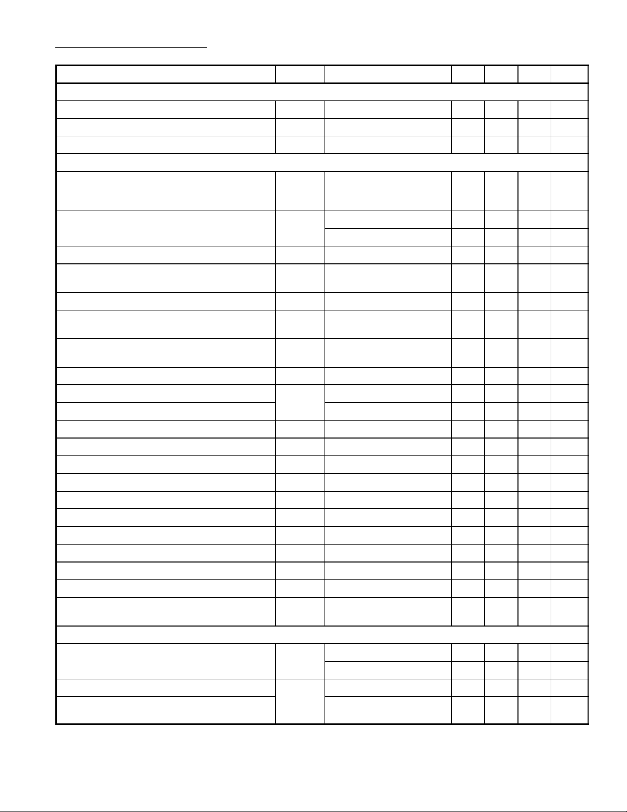
Electrical Characteristics: (VP = 14.5V, TA = +25°C, VFB = 45V, fi = 50Hz, I
otherwise specified)
Parameter Symbol Test Conditions Min Typ Max Unit
DC Supply
= 400µA unless
I(sb)
Operating Supply Voltage V
Flyback Supply Voltage V
Supply Current I
P
FB
No Signal, No Load – 30 55 mA
P
9.0 4.5 25.0 V
V
– 50 V
P
Vertical Circuit
Output Voltage Swing (Scan) V
Linearity Error LE IO = 2A
Output Voltage Swing (Flyback) V
Forward Voltage of the Internal Efficiency
Diode (V
O(A)
– VFB)
O(A)
– V
O(B)
V
V
Output Offset Current |IOS| I
Offset V oltage at the Input of the Feedback
Amplifier (V
I(fb)
– V
O(B)
)
Output Offset Voltage as a Function of
|VOS| I
∆VOST I
O
O
DF
I
= 0.6mA
diff
V
= 1.8V
diff
IO = 2A
(p–p)
(p–p)
IO = 50mA
I
= 0.3mA, IO = 1A (M) – 40 – V
diff
IO = –1A (M), I
= 0, I
diff
diff
diff
I(sb)
= 0, I
I(sb)
= 0 – – 72 µV/K
(p–p)
(p–p)
,
,
13.2 – – V
, Note 3 – 1 4 %
, Note 3 – 1 4 %
(p–p)
= 0.3mA – – 1.5 V
diff
= 50 to 500µA – – 40 mA
= 50 to 500µA – – 24 mV
Temperature
DC Output Voltage V
Open–Loop Voltage Gain (V
Open–Loop Voltage Gain (V
Voltage Ratio V
1–2/V9–4
7–4/V1–2
7–4/V9–4
) G
, V
= 0) Note 5 – 80 – dB
1–2
Frequency Response (–3dB) f
Current Gain (IO/I
) G
diff
O(A)Idiff
vo
V
R
res
I
= 0, Note 4 – 6.5 – V
Note 5, Note 6 – 80 – dB
– 0 – dB
Open Loop, Note 7 – 40 – Hz
– 5000 –
Current Gain Drift as a Function of Temperature ∆GcT – – 10
–4
K
Signal Bias Current I
Flyback Supply Current I
I(sb)
FB
During Scan – – 100 µA
50 400 500 µA
Power Supply Ripple Rejection PSRR Note 8 – 80 – dB
DC Input Voltage V
Common Mode Input Voltage V
Input Bias Current I
Common Mode Output Current I
I(DC)
I(CM)II(sb)
bias
O(CM)
I
I(sb)
∆I
fi = 50Hz, I
= 0 0 – 1.6 V
= 0 – 0.1 0.5 µA
I(sb)
= 300µA
diff
= 0
(p–p)
,
– 2.7 – V
– 0.2 – mA
Guard Circuit
Output Current I
Output Voltage on Pin8 V
O
O(guard)IO
Allowable Voltage on Pin8 Maximum Leakage
Not Active, V
Active, V
O(guard)
O(guard)
= 0V – – 50 µA
= 4.5V 1.0 – 2.5 mA
= 100µA – – 5.5 V
– – 40 V
Current = 10µA
 Loading...