

NTE NTE713 Datasheet
NTE713
Integrated Circuit
Chroma Demod
Description:
The NTE713 is a monolithic integrated circuit in a 14–Lead DIP type package that contains two sets
of synchronous detectors with matrix circuits to achieve the R–Y, G–Y, and B–Y color difference output
signals. The chroma input signal is applied to Pin3 and Pin4 while the oscillator injection signal is
applied to Pin6 and Pin7. The color difference signals, after matrix, have fixed a relationship of amplitude and phase nominally equal DC voltage levels. The outputs of the NTE713 are suitable for driving
high level color difference or R, G, B output amplifiers. Emitter–follower output stages used to drive
the high level color amplifiers have short–circuit protection.
Features:
D Synchronous Detector with Color Difference Matrix
D Emitter–Follower Output Amplifier with Short–Circuit Protection
Absolute Maximum Ratings:
(TA = +25°C unless otherwise specified)
DC Supply Voltage (Pin8 to Pin14) 27V. . . . . . . . . . . . . . . . . . . . . . . . . . . . . . . . . . . . . . . . . . . . . . . . . . .
Reference Input Voltage 5V
Chroma Input Voltage 5V
Device Dissipation (T
. . . . . . . . . . . . . . . . . . . . . . . . . . . . . . . . . . . . . . . . . . . . . . . . . . . . . . . . . . .
. . . . . . . . . . . . . . . . . . . . . . . . . . . . . . . . . . . . . . . . . . . . . . . . . . . . . . . . . . . . .
≤ +70°C) 530mW. . . . . . . . . . . . . . . . . . . . . . . . . . . . . . . . . . . . . . . . . . . . . . . . . .
A
Derate Linearly Above 70°C 6.7mW/°C. . . . . . . . . . . . . . . . . . . . . . . . . . . . . . . . . . . . . . . . . . . . .
Operating Ambient Temperature Range –40° to +85°C. . . . . . . . . . . . . . . . . . . . . . . . . . . . . . . . . . . . . .
Storage Temperature Range –65° to +150°C. . . . . . . . . . . . . . . . . . . . . . . . . . . . . . . . . . . . . . . . . . . . . . .
Lead Temperature (During Soldering, 1/32” from seating plane, 10sec max) +265°C. . . . . . . . . . . .
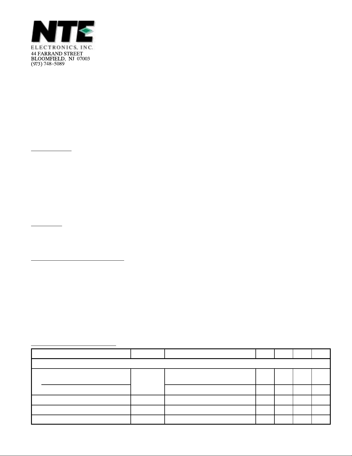
Electrical Characteristics:
Parameter Symbol Test Conditions Min Typ Max Unit
Static Characteristics
Supply Current
with Output Loads
With No Output Loads S1 Open – 9 – mA
G–Y, R–Y, B–Y Outputs V9, V11, V13S1 Closed 13.2 14.7 15.8 V
Chroma Inputs V3, V
Reference Subcarrier V6, V
(V+ = 24V, TA = +25°C unless otherwise specified)
I
T
S1 Closed 16.5 – 26.5 mA
S1 Open – 3.3 – V
4
S1 Open – 6.2 – V
7
P–P
P–P
Electrical Characteristics (Cont’d): (V+ = 24V, TA = +25°C unless otherwise specified)
Parameter Symbol Test Conditions Min Typ Max Unit
Dynamic Characteristics
Demodulator Unbalance v9, v11, v13V3 = V4 = 0 – – 0.8 v
Maximum Color Difference
Output Voltage
Chroma Input Sensitivity v
Relative R–Y Output v
Relative G–Y Output v
VDC Difference Between
Any Two Output Pins
Input Impedance
v
13
v
11
v
9
3
11
9
|V9| – |V11|
|V
| – |V13|
9
|V
| – |V13|
11
ri6, 7 – 1.7 – kΩ
Reference Subcarrier Inputs
Input Capacitance
ci6, 7 – 6 – pF
Reference Subcarrier Inputs
Input Impedance at Chroma Inputs ri3, 4 – 0.95 – kΩ
Input Capacitance at Chroma Inputs ci3, 4 – 5 – pF
Output Resistance ro9, ro11,
13
r
o
V3 = V4 = 0.6V
P–P
8.0 – – v
5.5 – – v
1.2 – – v
Adjust ec for 5v
@ Pin13 (B–Y) – 0.2 0.35 v
P–P
3.5 – 4.2 v
0.75 – 1.25 v
ec = 0 – – 0.6 V
– 180 – W
P–P
P–P
P–P
P–P
P–P
P–P
P–P
Pin Connection Diagram
1
N.C.
N.C.
(–) Chroma
(+) Chroma
2
3
4
5N.C.
6Ref “B”
7Ref “A”
14
GND
B – Y
13
12
N.C.
11
R – Y
10 N.C.
9 G – Y
8
V
CC
14 8
17
.785 (19.95)
Max
.200 (5.08)
Max
.300
(7.62)
.100 (2.45) .099 (2.5) Min
.600 (15.24)
 Loading...