

NTE NTE7126, NTE7125 Datasheet

NTE7125 & NTE7126
Integrated Circuit
Switching Regulator
Description:
The NTE7125 and NTE7126 are integrated circuits in a 12–Lead SIP type package incorporating all
the power switching, amplifier, error detection, and overcurrent protection circuits required in a self–
extcitation type semi–regulated off–line switching regulator. As a result, these devices can be used
in the design of switching power supplies with a minimal number of external components. Furthermore, the adoption of MOSFET power switching elements supports a higher oscillation frequency
than possible with bi–polar transistors. This allows smaller pulse transformers and capacitors to be
used, making it possible to construct miniature power supply systems.
Features:
D Power MOSFET Devices
D Ideal for Semi–Regulated Control Switching Supplies
D Error Detection Circuit On–Chip (40.5V ±0.5V Set Refernce Voltage)
D Overcurrent Protection Circuit On–Chip
D Higher Oscillation Frequency allows the use of Smaller Pulse Transformers
D IMST Substrate acts as an Electromagnetic Shield, makinf Low–Noise Designs Possible
Applications:
D CRT/CTV Power Supplies
D Office Automation Equipment Power Supplies
Absolute Maximum Ratings:
(TA = +25°C unless otherwise specified)
Operating Substrate Temperature (Recommended value is +105°C), TCmax +115°C. . . . . . . . . . . .
AC Input Voltage, V
OPerating Temperature Range, T
Storage Temperature Range, T
Maximum Output Power (V
. . . . . . . . . . . . . . . . . . . . . . . . . . . . . . . . . . . . . . . . . . . . . . . . . . . . . . . . . .
AC
opr
stg
= 135V), WOmax
O
–10° to +85°C. . . . . . . . . . . . . . . . . . . . . . . . . . . . . . . . . . . . . . . . .
–30° to +115°C. . . . . . . . . . . . . . . . . . . . . . . . . . . . . . . . . . . . . . . . . .
NTE7125 110W. . . . . . . . . . . . . . . . . . . . . . . . . . . . . . . . . . . . . . . . . . . . . . . . . . . . . . . . . . . . . . . . . .
NTE7126 145W. . . . . . . . . . . . . . . . . . . . . . . . . . . . . . . . . . . . . . . . . . . . . . . . . . . . . . . . . . . . . . . . . .
TR1
Drain Current, I
D
NTE7125 6A. . . . . . . . . . . . . . . . . . . . . . . . . . . . . . . . . . . . . . . . . . . . . . . . . . . . . . . . . . . . . . . . . . . . .
NTE7126 8A. . . . . . . . . . . . . . . . . . . . . . . . . . . . . . . . . . . . . . . . . . . . . . . . . . . . . . . . . . . . . . . . . . . . .
Pulse Drain Current, I
Drain Reverse Current, I
Gate–Source Voltage, V
D (pulse)
DR
GSS
140V
±30V. . . . . . . . . . . . . . . . . . . . . . . . . . . . . . . . . . . . . . . . . . . . . . . . . . . . . . . .
rms
20A. . . . . . . . . . . . . . . . . . . . . . . . . . . . . . . . . . . . . . . . . . . . . . . . . . . . . . . .
6A. . . . . . . . . . . . . . . . . . . . . . . . . . . . . . . . . . . . . . . . . . . . . . . . . . . . . . . . . . .
Absolute Maximum Ratings (Cont’d): (TA = +25°C unless otherwise specified)
TR1 (Cont’d)
Allowable Power Dissipation, P
D
Chip Junction Temperature, TJmax +150°C. . . . . . . . . . . . . . . . . . . . . . . . . . . . . . . . . . . . . . . . . . . . . . . .
Thermal Resistance, Junction–to–Case, R
thJ–C
ZD1
Allowable Power Dissipation, P
Chip Junction Temperature, T
Thermal Resistance, Junction–to–Case, R
ZD1
J (ZD1)
max +125°C. . . . . . . . . . . . . . . . . . . . . . . . . . . . . . . . . . . . . . . . . . . .
thJ–C (ZD1)
78.1W. . . . . . . . . . . . . . . . . . . . . . . . . . . . . . . . . . . . . . . . . . . . . . . . . . .
1.6°C/W. . . . . . . . . . . . . . . . . . . . . . . . . . . . . . . . . . . .
500mW. . . . . . . . . . . . . . . . . . . . . . . . . . . . . . . . . . . . . . . . . . . . . . .
0.2°C/W. . . . . . . . . . . . . . . . . . . . . . . . . . . . . . . .
Allowable Operating Ranges:
Pin4 Input Voltage, V
Oscillator Frequency, f
4
OSC
Operating Characteristics:
Parameter Symbol Test Conditions Min Typ Max Unit
Output Voltage Setting IIN = 8mA 40.0 40.5 41.0 V
Output Voltage Temperature Coefficient TC = 0° to +105°C, IIN = 8mA – 7 – mV/°
TR1
Drain–Source Breakdown Voltage V
Gate–Source Cutoff Voltage V
ON Resistance
NTE7125
NTE7126
Input Capacitance C
ZD1
Zener Voltage V
(TA = +25°C unless otherwise specified)
(TA = +25°C, TC = +25°C unless otherwise specified)
(BR)DSSID
GS(off)ID
R
DS(on)ID
iss
Z
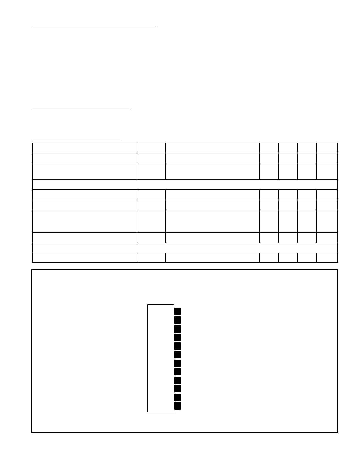
Pin Connection Diagram
= 10mA, VGS = 0V 500 – – V
= 1mA, VDS = 10V 2.0 – 3.0 V
= 2.5A, VGS = 10V
–
1.4
–
0.8
VDS = 10V, VGS = 0V, f = 1MHz – 800 – pF
IZ = 5mA 23.7 – 26.3 V
(Front View)
±6 to ±24V. . . . . . . . . . . . . . . . . . . . . . . . . . . . . . . . . . . . . . . . . . . . . . . . . . . . . . . .
20 to 120kHz. . . . . . . . . . . . . . . . . . . . . . . . . . . . . . . . . . . . . . . . . . . . . . . . . . .
1.8
1.8
C
Ω
Ω
TR1 Drain
12
11 TR1 Drain
10
No Pin
9
TR1 Source
8
TR1 Source
7
OCP Setting Level Input
6
Amplifier Circuit Control
5
TR1 Gate
Drive Voltage Input
4
GND
3
2
Error Detection Level
1
V
(40.5V typ) Input
ref
 Loading...