

NTE NTE7118 Datasheet

NTE7118
Integrated Circuit
Audio Power Amplifier, 50W
Description:
The NTE7118 integrated circuit is a hi–fi power amplifier in a 9–Lead SIP type package designed for
use as a building block in radio, TV, and other audio applications. The high performance of the IC
meets the requirements of digital sources (e.g. Compact Disc equipment).
The NTE7118 is totally protected, the two output transistors both having tthermal and SOAR protection. This device also has a mute function that can be arranged for a period after power–on with a
delay time fixed by external components.
The NTE7118 device is intended for symmetrical power supplies but an asymmetrical supply may
also be used.
Features:
D High Output Power (Also with Bootstrap)
D Low Offset Voltage
D Good Ripple Rejection
D Mute/Stand–by Facilities
D Thermal Protection
D Protected Against Electrostatic Discharge
D No Switch–On or Switch–Off Clicks
D Very Low Thermal Resistance
D Safe Operating Area (SOAR) Protection
D Short–Circuit Protection
Absolute Maximum Ratings:
Supply Voltage (Pin6 to Pin4), V
Bootstrap Voltage (Pin7 to Pin4), V
Output Current (Repetitive Peak), I
Mute Voltage (Pin3 to Pin4), V
Thermal Shut–Down Protection Time (Note 1), t
Storage Temperature Range, T
Thermal Resistance, Junction–to–Mounting Base, R
P
bstr
O
m
pr
stg
th j–mb
Note 1. Symmetrical power supply: AC and DC short–circuit protected.
Asymmetrical power supply: AC short–circuit protected.
Driven by a pink–noise voltage.
±30V. . . . . . . . . . . . . . . . . . . . . . . . . . . . . . . . . . . . . . . . . . . . . . . . . . .
70V. . . . . . . . . . . . . . . . . . . . . . . . . . . . . . . . . . . . . . . . . . . . . . . .
8A. . . . . . . . . . . . . . . . . . . . . . . . . . . . . . . . . . . . . . . . . . . . . . . . . . .
7V. . . . . . . . . . . . . . . . . . . . . . . . . . . . . . . . . . . . . . . . . . . . . . . . . . . . . . .
1 Hour. . . . . . . . . . . . . . . . . . . . . . . . . . . . . . . . . . .
–65° to +150°C. . . . . . . . . . . . . . . . . . . . . . . . . . . . . . . . . . . . . . . . . .
1K/W. . . . . . . . . . . . . . . . . . . . . . . . . . . . .
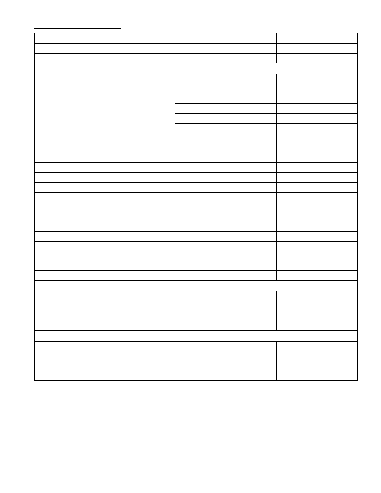
Electrical Characteristics: (VP = ±27.5V, RL = 8Ω, f = 1kHz, TA = +25°C unless otherwise specified)
Parameter Symbol Test Conditions Min Typ Max Unit
Supply Voltage Range (Pin6 to Pin4) V
Maximum Output Current (Peak Value) I
P
OMmax
Operating State
Input Voltage (Pin3 to Pin4) V
Total Quiescent Current I
Output Power P
3–4
tot
O
RL = ∞ 30 60 90 mA
THD = –60dB 37 40 – W
THD = –20dB – 51 – W
VP = ±23V, THD = –60dB, RL = 8Ω – 28 – W
VP = ±23V, THD = –60dB, RL = 4Ω – 50 – W
Total Harmonic Distortion THD PO = 32W – –90 –80 dB
Intermodulation Distortion d
PO = 32W, Note 2 – –80 – dB
im
Power Bandwidth B (–3dB) THD = –60dB 20 to 25,000 Hz
Slew Rate dV/dt – 10 – V/µs
Closed Loop Voltage Gain G
Open Loop Voltage Gain G
Note 3 – 30 – dB
c
o
Input Impedance |Zi| Note 4 1 – – MΩ
Signal–to–Noise Ratio S/N PO = 50mW, Note 5 80 – – dB
Output Offset Voltage V
Input Bias Current I
O
I
Output Impedance |Zo| – – 0.1 W
Supply Voltage Ripple Rejection SVRR Ripple Frequency = 100Hz,
Ripply Voltage = 500mV
eff
,
(RMS Value)
Source Resistance = 2kΩ
Quiescent Current into Pin2 I
Note 6 – – * µA
2
Mute State
Voltage on Pin3 V
Offset Voltage V
Output Voltage V
3–4
O
O
V
= 2V, f = 1kHz – 100 – µV
i(rms)
Ripple Rejection RR – 70 – dB
Standby State
Voltage on Pin3 V
Total Quiescent Current I
3–4
tot
Ripple Rejection RR – 70 – dB
Supply Voltage to Obtain Steady State ±V
P
±9 – ±30 V
6.4 – – A
6 – 7 V
– 85 – dB
– 2 * V
– 0.1 * µA
* – – dB
2 – 4.5 V
– * – V
0 – 1 V
– 20 – mA
4.5 – 7.0 V
* Value to be fixed.
Note 2. Measured with two superimposed signals of 50Hz and 7kHz with an amplitude relationship
of 4:1.
Note 3. The closed loop gain is determined by external resistors and is variable between 20dB and
46dB.
Note 4. The input impedance is determined by the bias resistor.
Note 5. The noise output voltage is measured in a bandwidth of 20Hz to 20kHz with a source resist-
ance of 2kΩ.
Note 6. The quiescent current into Pin2 has an impact on the mute time.
 Loading...