

NTE NTE7117 Datasheet
NTE7117
Integrated Circuit
Switched–Mode Power Supply Controller
Description:
The NTE7117 is a control circuit in an 8–Lead DIP type package designed for use in switched–mode
power supplies. It contains an internal temperature–compensated supply, PWM, sawtooth oscillator,
over–current sense latch, and output stage. This device is intended for low cost SMPS applications
where extensive housekeeping functions are not required.
Features:
D Pulse Width Modulator
D Current Limiting (Cycle–by–Cycle)
D Sawtooth Generator
D Stabilized Power Supply
D Double–Pulse Protection
D Internal Temperature–Compensated Reference
Applications:
D Switch–Mode Power Supplies
D DC Motor Controller Inverter
D DC/DC Converter
Absolute Maximum Ratings:
Supply Voltage, V
Output Current, I
CC
OUT
Output Duty Cycle 98%. . . . . . . . . . . . . . . . . . . . . . . . . . . . . . . . . . . . . . . . . . . . . . . . . . . . . . . . . . . . . . . . .
Maximum Total Power Dissipation, P
Operating Temperature Range, T
A
D
750mW. . . . . . . . . . . . . . . . . . . . . . . . . . . . . . . . . . . . . . . . . . . . .
0° to +70°C. . . . . . . . . . . . . . . . . . . . . . . . . . . . . . . . . . . . . . . . . . . . .
DC Electrical Characteristics: (VCC = 12V, TA = +25°C unless otherwise specified)
Parameter Symbol Test Conditions Min Typ Max Unit
Reference Section
Internal Reference Voltage V
Internal Zener Reference V
Temperature Coefficient of V
Temperature Coefficient of V
Oscillator Section
Frequency Range f TA = 0° to +70°C 50 – 100k Hz
Initial Accuracy RT and CT Constant – 5 – %
Duty Cycle Range fo = 20kHz 0 – 98 %
REF
Z
REF
Z
TA = +25°C 3.69 3.75 3.84 V
TA = 0° to +70°C 3.66 – 3.87 V
IL = 7mA 7.8 8.2 8.8 V
– ±100 – ppm/°C
– ±100 – ppm/°C
18V. . . . . . . . . . . . . . . . . . . . . . . . . . . . . . . . . . . . . . . . . . . . . . . . . . . . . . . . . . . . . . . .
40mA. . . . . . . . . . . . . . . . . . . . . . . . . . . . . . . . . . . . . . . . . . . . . . . . . . . . . . . . . . . . . .
DC Electrical Characteristics (Cont’d): (VCC = 12V, TA = +25°C unless otherwise specified)
Parameter Symbol Test Conditions Min Typ Max Unit
Current Limiting
Input Current I
Single Pulse Inhibit Delay
Current Limit Trip Level 0.4 0.5 0.6 V
Error Amplifier
Open–Loop Gain – 60 – dB
Feedback Resistor 10k – – Ω
Small–Signal Bandwidth BW – 3 – MHz
Output Voltage Swing, High V
Output Voltage Swing, Low V
Output Stage
Output Current I
Saturation Voltage V
Supply Voltage/Current
Supply Current I
Supply Voltage V
Low Supply Protection
Pin1 Threshold 8.0 9.0 10.5 V
OUT
IN
OH
OL
CE
CC
CC
Pin6 = 250mV TA = +25°C – –2 –10 µA
TA = 0° to +70°C – – –20 µA
I
Inhibit Delay Time
for 20% Overdrive
TA = 0° to +70°C 20 – – mA
TA = 0° to +70°C IC = 20mA – – 0.4 V
IZ = 0,
Voltage–Fed
IS = 10mA, Current–Fed 19 21 24 V
ICC = 30mA, Current–Fed 20 – 30 V
= 20mA – 0.88 1.10 µs
OUT
I
= 40mA – 0.7 0.8 µs
OUT
6.2 – – V
– – 0.7 V
IC = 40mA – – 0.5 V
TA = +25°C – – 10 mA
TA = 0° to +70°C – – 13 mA
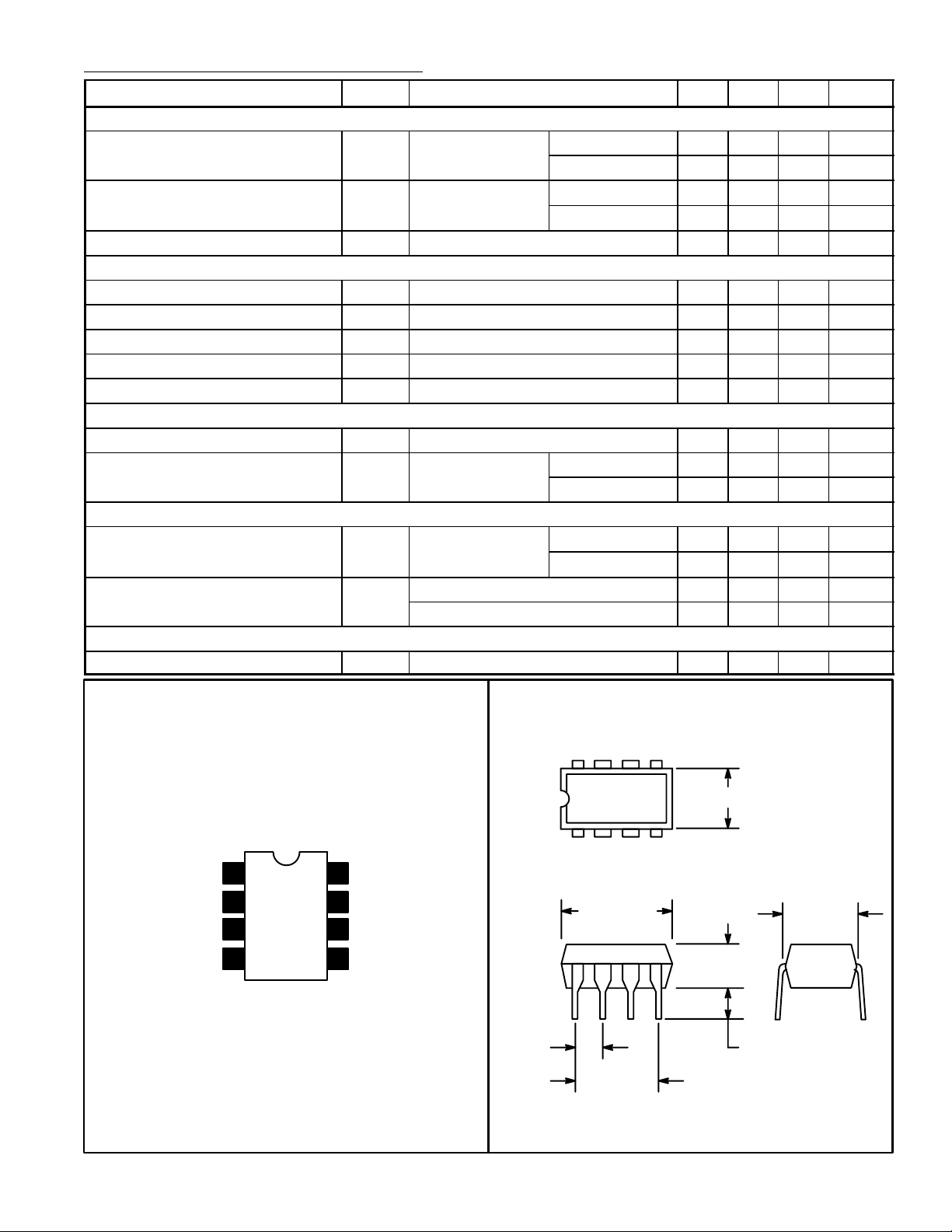
Pin Connection Diagram
V
CC
V
Feedback
85
.256 (6.52) Max
14
1
2
Z
3
4Gain
GND
8
Output
7
6
Current Sense
5
RT, C
T
(2.54)
.393 (10.0)
Max
.300 (7.62)
.300
(7.62)
.150
(3.81)
.070 (1.77) Min.100
 Loading...