

NTE NTE7116 Datasheet

NTE7116
Integrated Circuit
Phase Lock Loop (PLL) Stereo Decoder
(BTSC System)
Description:
The NTE7116 is a phase lock loop (PLL) stereo decoder in a 20–Lead DIP type package designed
primarily for low cost stereo decoding in a low–to–medium–line TV. The MUX input (Pin1) is a low
impedance current input, the gain of the input amplifier is therefore determined by the external resistor
R1. All characteristics are measured with R1 = 47kΩ. The de–emphasis of (L, R) and (L – R) can
be chosen by means of external capacitors and resistors. The supply voltage range of the device is
from 7V to 16V.
Features:
D Wide Supply Voltage Range
D Automatic Mono/Stereo Switching (Pilot Presence Detector)
D LED Driver for Stereo Indicator
D Smooth Mono/Stereo Control
D Matrix and Two Amplifiers for Left and Right Output Signals
D A Source Selector to Switch between the MUX Signal and an External Signal
D Mute Circuit for 60dB Muting of the Output Level
D External De–Emphasis Control of (L, R) and (L – R)
D 6dB Fixed Attenuation of (L – R) with respect to (L + R) Prior to Matrix
D All Pins are Protected Against Electrostatic Discharge (ESD)
Absolute Maximum Ratings:
Supply Voltage Range (Pin5), V
LED Driver Current (Peak Value), I
Total Power Dissipation (T
Electrostatic Handling, V
A
es
P
3
= +25°C), P
tot
Operating Ambient Temperature Range, T
Storage Temperature Range, T
stg
18V. . . . . . . . . . . . . . . . . . . . . . . . . . . . . . . . . . . . . . . . . . . . . . . . . . . . .
75mA. . . . . . . . . . . . . . . . . . . . . . . . . . . . . . . . . . . . . . . . . . . . . . . .
1.9W. . . . . . . . . . . . . . . . . . . . . . . . . . . . . . . . . . . . . . . . . . . .
–2 to +2kV. . . . . . . . . . . . . . . . . . . . . . . . . . . . . . . . . . . . . . . . . . . . . . . . . . . . .
A
0° to +70°C. . . . . . . . . . . . . . . . . . . . . . . . . . . . . . . . . . . . .
–65° to +150°C. . . . . . . . . . . . . . . . . . . . . . . . . . . . . . . . . . . . . . . . . .
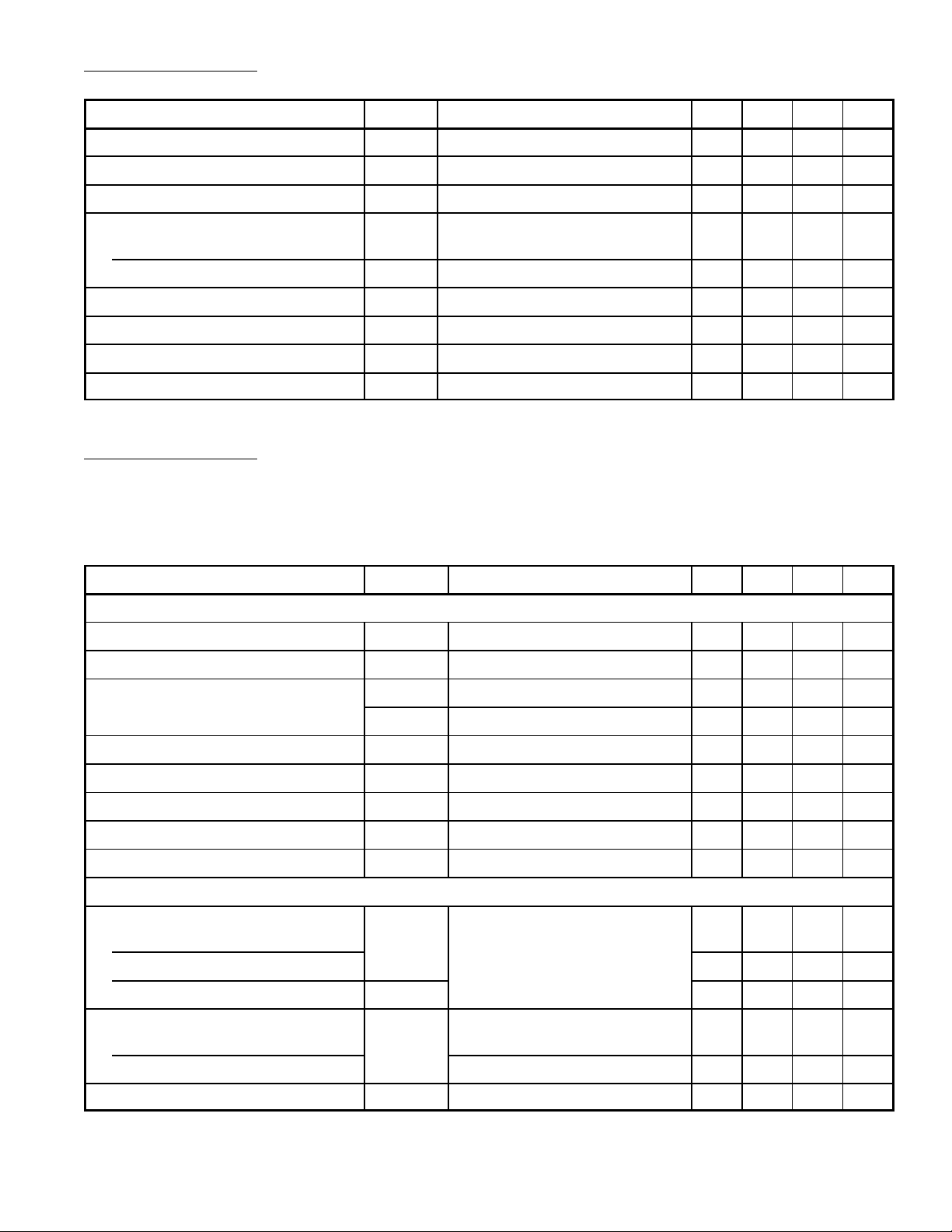
DC Characteristics: (VS = 8.5V, TA = +25°C, all voltages are with respect to GND (Pin20), all
currents are positive into the device unless otherwise specified)
Parameter Symbol Test Conditions Min Typ Max Unit
Supply Voltage V
Total Current Consumption I
Power Dissipation P
tot
tot
S
Without LED Driver – 19 25 mA
7.0 8.5 16.0 V
– 160 – mW
Voltage
Pin1
Pins 8, 9, 10, 11, 12, & 13 V
DC Output Current (Pin14 & Pin15) –I14, I
LED Driver Current (Pin3) I
Switch “VCO–OFF” Voltage V
Switch “VCO–OFF” Current I
V
1
8–13
3
19
19
– 2.1 – V
– 4.2 – V
15
1.1 1.4 1.8 mA
– – 20 mA
I19 = 50µA – 2 – V
50 – – µA
AC Characteristics: (VS = 8.5V, TA = +25°C, AC Conditions: (1) Input signal (Vi) of 815mV
L = 1, R = 1 (mono), f
of 1.2V
for L = 1, R = 0 and no dbx, fm = 1kHz (stereo) and V
P–P
= 1kHz (80% modulation); (2) MUX input signal (Vi)
m
= 200V
pilot
(3) S1 open, unless specified (without L – R filter), VCO measured with an
external IF roll–of f network (–2dB at 31.5kHz = 2f
) at the input. All the above
H
conditions apply unless otherwise specified)
Parameter Symbol Test Conditions Min Typ Max Unit
P–P
for
P–P
;
Overall Performance Vi to V
Input Current (rms) I
Overall gain G
AF Output Voltage (rms) V11 = V
o
(rms)
O
V15 = V
Mono; R1 = 47kΩ 4.0 5.8 7.0 dB
10
14
– – 12 µA
460 560 640 mV
– 245 – mV
Total Harmonic Distortion THD Note 1 – 0.3 0.5 %
Output Voltage V11 = V10THD = 1% – 800 – mV
Output Channel Unbalance V11/V
10
– 0.1 1.0 dB
Channel Separation α L = 1, R = 0 24 28 – dB
Signal to Noise Ratio S/N Bandwidth 20Hz to 16kHz – 76 – dB
Pilot Presence Detector (Note 2)
Switching to
Stereo
V
pilot
– 40 60 mV
Mono 15 30 – mV
Hysteresis ∆V
Channel Separation
Full Stereo
pilot
α
V16 ≥ 1.25V
– 2.5 – dB
24 28 – dB
Smooth Operation V16 = 1V Typ – 10 – dB
Attenuation (L – R) – 6 – dB
Note 1. Guaranteed for mono, mono + pilot and stereo.
Note 2. Adjustable.
 Loading...