

NTE NTE7115 Datasheet

NTE7115
Integrated Circuit
Color TV Horizontal Combination Circuit
Description:
The NTE71115 is a monolithic integrated circuit in a 18–Lead DIP type package designed for use in
color television receivers.
Features:
D Positive Video Input: Capacitively Coupled (Source Impedance < 200Ω)
D Adaptive Sync Separator: Slicing Level at 50% of Sync Amplitude
D Internal Vertical Pulse Separator
D Output Stage for Vertical Sync Pulse or Composite Sync Depending on the Load; Both are
Switched OFF at Muting
D ö
D Coincidence Detector ö
Phase Control Between Horizontal Sync and Oscillator
1
for Automatic Time Constant Switching; Overruled by the VCR Switch
3
D Time Constant Switch Between Two External Time Constants for Loop Gain; Both Controlled
by the Coincidence Detector ö
D ö
Gating Pulse Controlled by Coincidence Detector ö
1
D Mute Circuit Depending on TV Transmitter Identification
D ö
Phase Control Between Line Flyback and Oscillator; the Slicing Levels for ö2 Control and
2
Horizontal Blanking can be set Separately
D Burst Keying and Horizontal Blanking Pulse Generation, in Combination with Clamping of the
Vertical Blanking Pulse (Three–Level Sandcastle)
D Horizontal Drive Output with Constant Duty Cycle Inhibited by the Protection Circuit or the
Supply Voltage Sensor
D Detector for Too Low Supply Voltage
D Protection Circuit for Switching Off the Horizontal Drive Output Continuously if the Input Voltage
is Below 4V or Higher than 8V
D Line Flyback Control Causing the Horizontal Blanking Level at the Sandcastle Output Continuously
in Case of a Missing Flyback Pulse
D Spot Suppressor Controlled by the Line Flyback Control
w
/Double Slope Integrator
3
3
Applications:
D Television Receivers
D Video Receivers
Absolute Maximum Ratings:
Supply Voltage (Pin19), V
15–5
= V
CC
Voltages at:
(Pin1, Pin4, and Pin7), V
(Pin8, Pin13, and Pin18), V
(Pin11 (Range)), V
11–5
1–5
, V
8–5
4–5
, V
, V
13–5
Currents at:
Pin1, I
Pin2 (Peak Value), ±I
Pin4, I
Pin6 (Peak Value), ±I
Pin7, I
Pin8 (Range), I
Pin9 (Range), I
Pin18, ±I
Total Power Dissipation, P
1
2M
4
6M
7
8
9
18
TOT
Operating Ambient Temperature Range, T
Storage Temperature Range, T
stg
A
7–5
, V
. . . . . . . . . . . . . . . . . . . . . . . . . . . . . . . . . . . . .
18–5
13.2V. . . . . . . . . . . . . . . . . . . . . . . . . . . . . . . . . . . . . . . . . . . . . . . .
18V. . . . . . . . . . . . . . . . . . . . . . . . . . . . . . . . . . . . . . . . .
V
CC
–0.5 to +6.0V. . . . . . . . . . . . . . . . . . . . . . . . . . . . . . . . . . . . . . . . . . . . . . .
10mA. . . . . . . . . . . . . . . . . . . . . . . . . . . . . . . . . . . . . . . . . . . . . . . . . . . . . . . . . . . . . . . . . . .
10mA. . . . . . . . . . . . . . . . . . . . . . . . . . . . . . . . . . . . . . . . . . . . . . . . . . . . .
100mA. . . . . . . . . . . . . . . . . . . . . . . . . . . . . . . . . . . . . . . . . . . . . . . . . . . . . . . . . . . . . . . . . .
6mA. . . . . . . . . . . . . . . . . . . . . . . . . . . . . . . . . . . . . . . . . . . . . . . . . . . . . .
10mA. . . . . . . . . . . . . . . . . . . . . . . . . . . . . . . . . . . . . . . . . . . . . . . . . . . . . . . . . . . . . . . . . . .
–5 to +1mA. . . . . . . . . . . . . . . . . . . . . . . . . . . . . . . . . . . . . . . . . . . . . . . . . . . . . . .
–10 to +3mA. . . . . . . . . . . . . . . . . . . . . . . . . . . . . . . . . . . . . . . . . . . . . . . . . . . . . .
10mA. . . . . . . . . . . . . . . . . . . . . . . . . . . . . . . . . . . . . . . . . . . . . . . . . . . . . . . . . . . . . . . .
800mW. . . . . . . . . . . . . . . . . . . . . . . . . . . . . . . . . . . . . . . . . . . . . . . . . . . .
–0° to +70°C. . . . . . . . . . . . . . . . . . . . . . . . . . . . . . . . . . . .
–65° to +150°C. . . . . . . . . . . . . . . . . . . . . . . . . . . . . . . . . . . . . . . . . .
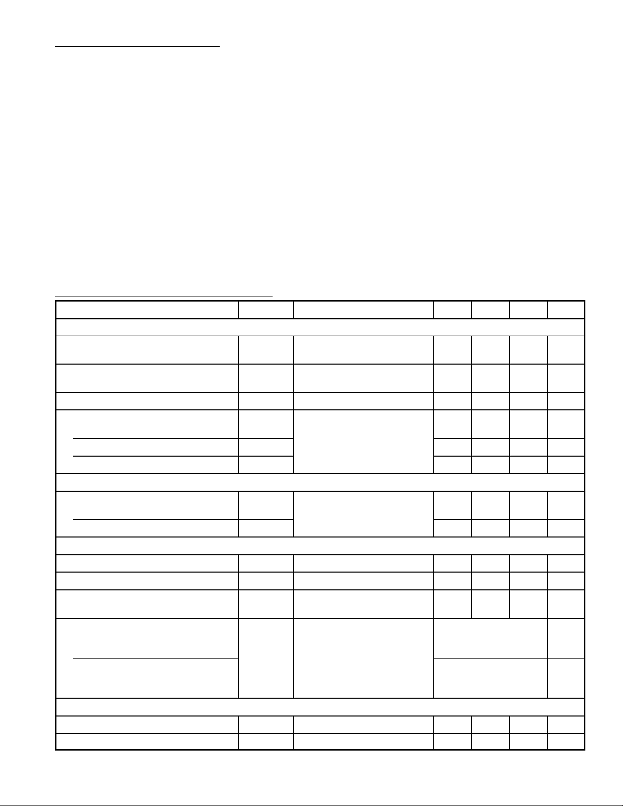
DC and AC Electrical Characteristics:
Parameter Symbol Test Conditions Min Typ Max Unit
Composite Video Input and Sync Separator, Pin11 (Internal Black Level Determination)
Input Signal (Positive Video; Standard
Signal; Peak–to–Peak Value)
Sync Pulse Amplitude (Independent of
Video Content)
Generator Resistance R
Input Current During
Video
Sync Pulse –I
Black Level –I
Composite Sync Generation, Pin10 (Horizontal Slicing Level at 50% of the Sync Pulse Amplitude)
Capacitor Current During
Video
Sync Pulse –I
Vertical Sync Pulse Generation, Pin9 (Slicing Level at 30% (60% Between Black Level and Horizontal Slicing Level))
Output Voltage V
Pulse Duration t
Delay With Respect to the V ertical Sync
Pulse (LeadinG Edge)
Pulse–Mode Control
Output Current for Vertical Sync
Pulse (Dual Integrated)
(VCC = 12V, TA = +25°C unless otherwise specified)
V
11–5(P–P)
V
11–5(P–P)
I
11
I
10
10
9–5
p
t
D
G
11
11
0.2 1.0 3.0 V
50 – – mV
– – 200 Ω
– 5 – µA
– 40 – µA
– 25 – µA
– 16 – µA
– 170 – µA
10 – – V
– 190 – µs
– 45 – µs
No Current Applied
at Pin9
Output Current for Horizontal and
Vertical Sync Pulse (Non–Inte-
grated Separated Signal)
Horizontal Oscillator, Pin14 and Pin16
Free–Running Frequency f
Reference Voltage for f
OSC
V
OSC
14–5
Current Applied Via a
15kΩ from V
– 15.625 – kHz
– 6 – V
to Pin9
CC
 Loading...