

NTE NTE7110 Datasheet
NTE7110
Integrated Circuit
3 Channel Analog Switch
Description:
The NTE7110 is an integrated circuit in a 16–Lead DIP type package designed for use as an electronic
switch in VCR and audio signal processing applications. This device contains three channel two input
switch circuits with each switch being controlled independently.
Features:
D Low Offset Voltage at Output: 5mV Typ
D Low Switching Noise
D Wide Dynamic Range
D Wide Frequency Range: 40MHz Typ
D Low Crosstalk
D High Speed Response: 0.2µs Typ
D Low Power Consumption
Absolute Maximum Ratings:
Supply Voltage, V
Power Dissipation, P
CC
D
Derate Above 25°C 10mW/°C. . . . . . . . . . . . . . . . . . . . . . . . . . . . . . . . . . . . . . . . . . . . . . . . . . . . . .
Operating Temperature Range, T
Storage Temperature Range, T
stg
opr
–20° to +75°C. . . . . . . . . . . . . . . . . . . . . . . . . . . . . . . . . . . . . . . . .
–40° to +125°C. . . . . . . . . . . . . . . . . . . . . . . . . . . . . . . . . . . . . . . . . .
14V. . . . . . . . . . . . . . . . . . . . . . . . . . . . . . . . . . . . . . . . . . . . . . . . . . . . . . . . . . . . . . . .
1000mw. . . . . . . . . . . . . . . . . . . . . . . . . . . . . . . . . . . . . . . . . . . . . . . . . . . . . . . . . .
Recommended Operating Condition:
Supply Voltage Range, V
Electrical Characteristics:
Parameter Symbol Test Conditions Min Typ Max Unit
Circuit Current I
Voltage Gain G
CC
(TA = +25°C unless otherwise specified)
CC1
I
CC2
V1
G
V2
4.5V to 13V. . . . . . . . . . . . . . . . . . . . . . . . . . . . . . . . . . . . . . . . . . . . . . . . . .
VCC = 9V 5.2 7.1 9.0 mA
VCC = 5V 2.4 3.4 4.4 mA
f = 1MHz, Vin = 0.5V
f = 10MHz, Vin = 0.5V
P–P
P–P
–0.6 –0.1 0.4 dB
–0.6 –0.1 0.4 dB
Electrical Characteristics (Cont’d): (TA = +25°C unless otherwise specified)
Parameter Symbol Test Conditions Min Typ Max Unit
2nd Harmonic Distortion HD f = 5MHz, Vin = 4.5V
Switch Crosstalk CT
Channel Crosstalk CT
Output DC Offset Voltage V
Switch Threshold Voltage V
V
V
Input Impedance Z
Control Input 1
Control Input 3
OS
th1
th2
th3
f = 5MHz, Vin = 0.5V
sw
f = 5MHz, Vin = 0.5V
ch
VCC = 5V 1.3 – 2.3 V
VCC = 9V 1.7 – 2.7 V
VCC = 12V 2.0 – 3.0 V
in
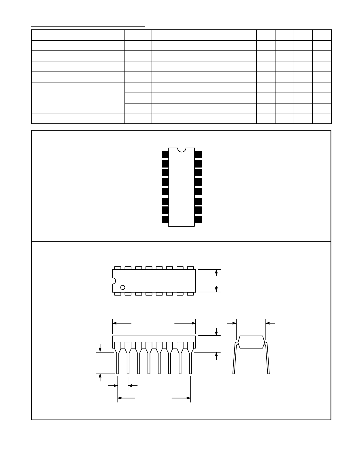
Pin Connection Diagram
Input 1B
Output 1
GND 2
Output 2
Output 3
Input 3A
1
2
3
4
5
6
7
8
Input 1A
16
15
GND 1
Input 2B
14
V
13
Control Input 2
12
11
Input 2A
GND 3
10
Input 3B
9
, RL = 2kΩ – –60 –50 dB
P–P
P–P
P–P
– –70 –60 dB
– –70 –60 dB
–10 0 +10 mV
– 20 – kΩ
CC
.245
(6.22)
Min
16 9
.260 (6.6) Max
18
.785 (19.9)
Max
.200 (5.08)
Max
.100 (2.54)
.700 (17.7)
.300
(7.62)
 Loading...