

NTE NTE7104, NTE7039 Datasheet
NTE7039 & NTE7104
Integrated Circuit
Vertical Deflection Output Circuit
w
/Drive Circuit for CRT Display
Description:
The NTE7039 and NTE7104 are vertical deflection output ICs developed for use in high–grade TVs
and displays. The interlace and crossover distortion responses, in particular , have been greatly improved, allowing excellent picture quality on large size television screens and high precision interlace
mode displays.
Also, pulse signals can be used for input signals due to the on–chip sawtooth wave generating circuit
and driver circuit. Further, the DC and AC feedback circuits can be formed with these ICs alone, simplyfing pattern design of sets and ensuring stable performance.
The NTE7104 has a maximum deflection current of 1.8A
, making it appropriate for use in portable
p–p
to mid–size televisions while the NTE7039 has a minimum deflection current of 2.2A
used for larger size sets, and can drive television screen sizes from 33 to 37 inches.
Features:
D Low Power Dissipation due to On–Chip Pump–Up Circuit
D On–Chip 50/60Hz Vertical Size Control Circuit
D On–Chip Sawtooth Wave Generating Circuit
D On–Chip Drive Circuit
D Vertical Output Circuit
D On–Chip Thermal Protection Circuit
D Excellent Interlace Response
D Excellent Crossover Response
Absolute Maximum Ratings:
Driver Supply Voltage, +V
Pump–Up Supply Voltage, +V
Output Supply Voltage, +V
Deflection Output Current, I
Thermal Resistance, Junction–to–Case, R
Allowable Power Dissipation (With Infinite Heat Sink), P
Operating Temperature Range, T
Storage Temperature Range, T
(TA = +25°C unless otherwise specified)
1 max 15V. . . . . . . . . . . . . . . . . . . . . . . . . . . . . . . . . . . . . . . . . . . . . . . . . . .
CC
8 max 30V. . . . . . . . . . . . . . . . . . . . . . . . . . . . . . . . . . . . . . . . . . . . . . . .
CC
13 max 62V. . . . . . . . . . . . . . . . . . . . . . . . . . . . . . . . . . . . . . . . . . . . . . . . . .
CC
. . . . . . . . . . . . . . . . . . . . . . . . . . . . . . . . . . . . . . . . . .
DEF
thJ–C
max 8W. . . . . . . . . . . . . . . . . . . . . . . . . . .
D
opr
stg
–1.5 to +1.5A
, so it can be
p–p
–20° to +85°C. . . . . . . . . . . . . . . . . . . . . . . . . . . . . . . . . . . . . . . . .
–40° to +150°C. . . . . . . . . . . . . . . . . . . . . . . . . . . . . . . . . . . . . . . . . .
P–O
4°C/W. . . . . . . . . . . . . . . . . . . . . . . . . . . . . . . . . . . . . .
Recommended Operating Conditions: (TA = +25°C unless otherwise specified)
Parameter Symbol Min Typ Max Unit
Driver Supply Voltage +VCC1 8 12 14 V
Pump–Up Supply Voltage +VCC8 10 24 27 V
Deflection Output Current
NTE7039
NTE7104 up to 1.8 A
Ramp Waveform Pulse Height
NTE7039
NTE7104 up to –1.01 V
I
12p–p
V
6p–p
up to 2.2 A
up to +B1/3 V
p–p
p–p
p–p
p–p
Electrical Characteristics: (TA = +25°C, +VCC1 = 12V, +VCC8 = 24V unless otherwise specified)
Parameter Symbol Test Conditions Min Typ Max Unit
Driver Supply Current ICC1 5.6 6.7 7.8 mA
Trigger Input Threshold Voltage V
Vertical Amplitude Control Pin Voltage V
Ramp Waveform Generator Start Voltage V
Pump–Up Charge Saturation Voltage V
Pump–Up Discharge Saturation Voltage
NTE7039
RAMP
S9–11
V
S8–9
2
4
I9 = 20mA – – 1.8 V
I = 1.1A – – 3.2 V
NTE7104 I = 0.9A – – 3.0 V
Deflection Output Saturation Voltage (Lower)
NTE7039
V
S12–11
I = 1.1A – – 1.5 V
NTE7104 I = 0.9A – – 1.2 V
2.6 2.9 3.2 V
5.9 6.1 6.3 V
4.6 4.9 5.2 V
Deflection Output Saturation Voltage (Upper)
NTE7039
V
S13–12
I = 1.1A – – 3.5 V
NTE7104 I = 0.9A – – 3.2 V
Idling Current I
DL
35 – 65 mA
Voltage Gain – 59 – dB
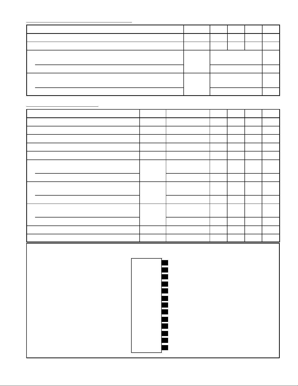
Pin Connection Diagram
(Front View)
Power Supply for
13
Vertical Output
Vertical Output
12
11
GND
OSC Stop
10
9
Pump–Up Output
+VCC8
8
Vertical Output
7
AC/DC Feedback
6
Ramp Generator
5
Vertical Size Control
4
Vertical Amp Control
Time Constant
3
2
Vertical T rigger Input
+V
CC
1
1
 Loading...