

NTE NTE7103 Datasheet

NTE7103
Integrated Circuit
50W to 80W Power Amplifier, Driver
Description:
The NTE7103 is an integrated monolithic circuit in a 14–Lead SIP type package designed for use in
50W to 80W class HiFi audio power amplifier applications. This device consists of an input differential
amplifier, a predriver circuit, a driver circuit, and an over current protection circuit.
Features:
D Low Distortion
0.002% Typ. (V
0.006% Typ. (V
D Wide Frequency Band
D Wide Power Band
= ±46V, f = 1kHz, Av = 30dB, PO = 50W, RL = 8Ω w/Power Transistor)
CC
= ±46V, f = 20kHz, Av = 30dB, PO = 50W, RL = 8Ω w/Power Transistor)
CC
Absolute Maximum Ratings:
Supply Voltage (Quiescent), V
Supply Voltage (Operational), V
Circuit Current, I
(peak) 250mA. . . . . . . . . . . . . . . . . . . . . . . . . . . . . . . . . . . . . . . . . . . . . . . . . . . . . . . .
CC
(TA = +25°C unless otherwise specified)
CC1
CC2
Allowable Package Dissipation (Note 1), P
Operating Temperature Range, T
Storage Temperature Range, T
opr
stg
Note 1. 100 x 100 x 2mm Al heat sink.
Recommended Operating Conditions:
Supply Voltage (Operational), V
Input Bias Resistance, R
Power Transistor h
FE
IN
(PO = 80W, RL = 8Ω, TJ < +125°C), h
Closed Loop Voltage Gain, A
Junction Temperature Range, T
CC
v
J
±65V. . . . . . . . . . . . . . . . . . . . . . . . . . . . . . . . . . . . . . . . . . . . . . . . . . .
±50V. . . . . . . . . . . . . . . . . . . . . . . . . . . . . . . . . . . . . . . . . . . . . . . . . .
D
7.5W. . . . . . . . . . . . . . . . . . . . . . . . . . . . . . . . . . . . . . . . . .
–20° to +75°C. . . . . . . . . . . . . . . . . . . . . . . . . . . . . . . . . . . . . . . . .
–40° to +150°C. . . . . . . . . . . . . . . . . . . . . . . . . . . . . . . . . . . . . . . . . .
±20 to ±46V. . . . . . . . . . . . . . . . . . . . . . . . . . . . . . . . . . . . . . . . . . . . .
1 to 50 to 100kΩ. . . . . . . . . . . . . . . . . . . . . . . . . . . . . . . . . . . . . . . . . . . . . . . .
FE
≤ 50. . . . . . . . . . . . . . . . . . . . . . . . . . .
26 to 30dB. . . . . . . . . . . . . . . . . . . . . . . . . . . . . . . . . . . . . . . . . . . . . . . . . .
–20° to +125°C. . . . . . . . . . . . . . . . . . . . . . . . . . . . . . . . . . . . . . . . . . .
Electrical Characteristics: (VCC = ±46V, Av = 30dB, TA = +25°C unless otherwise specified)
Parameter Symbol Test Conditions Min Typ Max Unit
Output Offset Voltage V
offset
Quiescent Circuit Current I
Maximum Output Voltage V
Open Loop Voltage Gain A
Output Noise Voltage V
Rolloff Frequency f
CC
OM
VIN = 0 – ±5 ±50 mV
VIN = 0 – 20 40 mA
THD = 0.05%, f = 20Hz to 20kHz 25 28 – V
VO = 1.5V, f = 1kHz 80 95 – dB
vo
RG = 10kΩ – 0.07 0.14 mV
n
VO = 1.5V, –3dB – 900 – kHz
H
Supply Voltage Rejection Ratio SVR RG = 2.2kΩ, f
v
= 1V
ripple
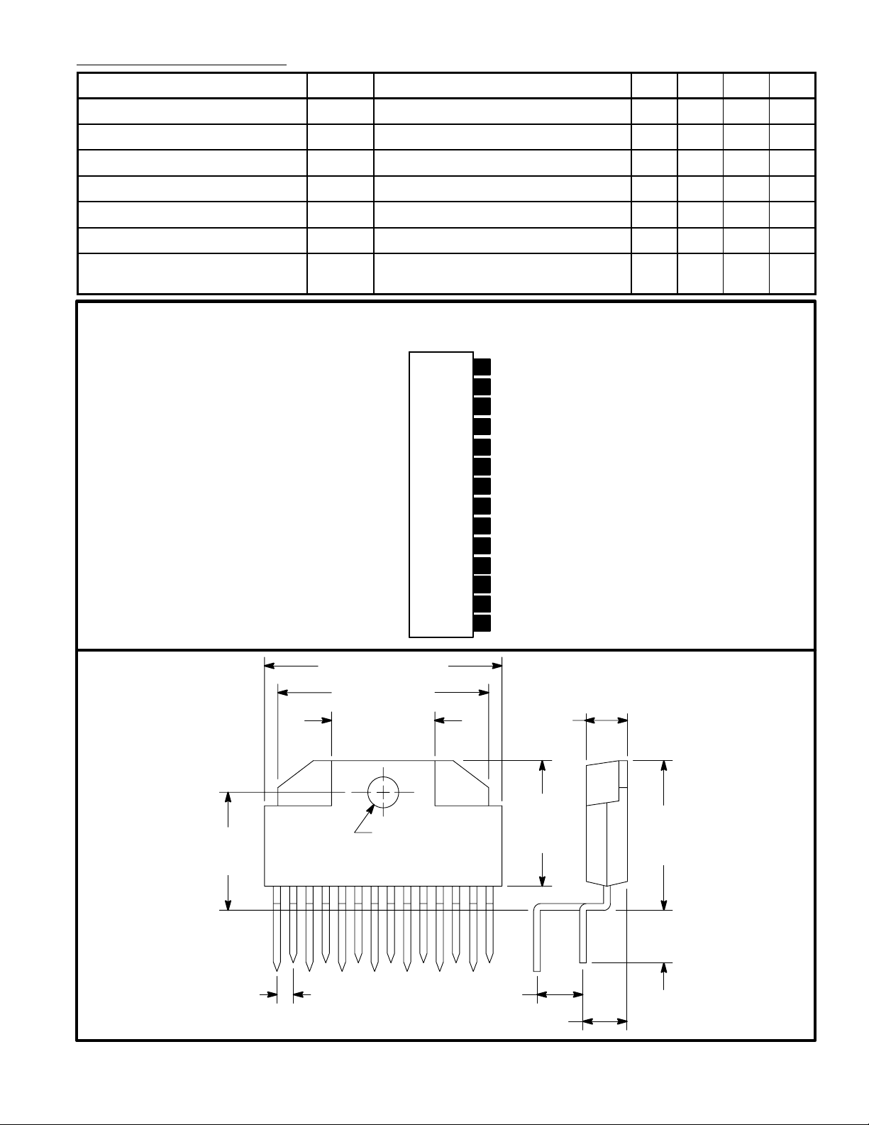
Pin Connection Diagram
(Front View)
rms
= 100Hz,
ripple
N.C.
14
N.C.
13
12
Upper Output
11
Lower Output
10
–V
(for Driver)
CCD
–V
9
8
7
6
5
4
3
+V
2
+V
1
(for Preamp)
CCP
Bias
Bias
Phase Compensation
NFB
Input
Muting
(for Preamp)
CCP
(for Driver)
CCD
55 70 – dB
.480
(12.2)
1.000 (25.4) Max
.843 (21.4)
.472 (12.0)
.142 (3.6) Dia.
114
.067 (1.7) Max .200 (5.08)
.138
(3.5)
.532
(13.5)
Max
.138 (3.5)
.607
(15.4)
Max
.134
(3.4)
 Loading...