

NTE NTE7101 Datasheet
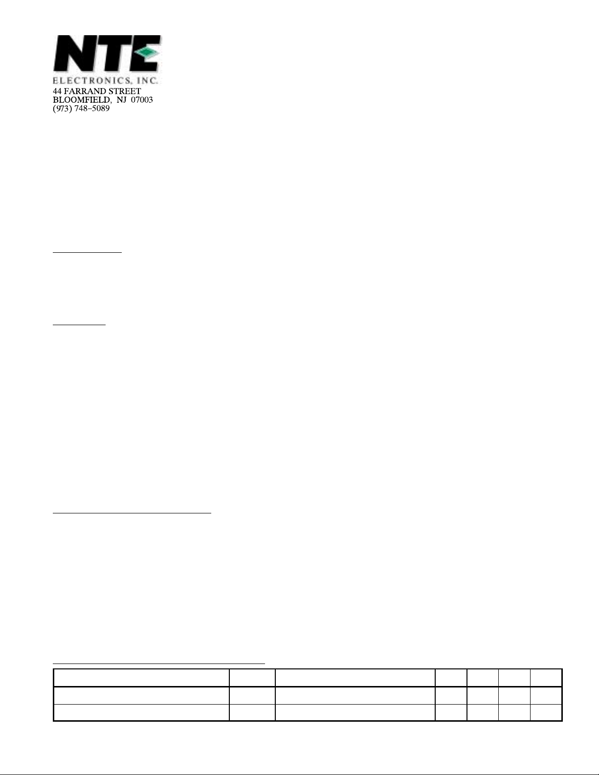
NTE7101
Integrated Circuit
AF Power Amplifier, 7W
Description:
The NTE7101 is an audio power amplifier in an 8–Lead SIP type package designed for use in car radio
and car stereo applications. This device features a low thermal resistance providing easy design for
2Ω load circuits and 4Ω load BTL circuits.
Features:
D High Output Power:
P
= 7W Typ @ RL = 4Ω, THD = 10%, VCC = 14.4V
O
= 11W Typ @ RL = 2Ω, THD = 10%, VCC = 14.4V
P
O
P
= 18W (Bridge) @ RL = 4Ω, THD = 10%, VCC = 14.4V
O
D Low Distortion: THD = 0.1% Typ @ R
D High Reliability
D Protection Circuits Include:
Load Dump Voltage Surge
Thermal Overload
Output DC and AC Short Circuit to GND or V
Reverse Insertion
D Minimum External Components Required
= 4Ω, PO = 500mW
L
CC
Absolute Maximum Ratings:
Surge Supply Voltage (PW = 200ms), V
Quiescent Supply Voltage (Note 1), V
(TA = +25°C unless otherwise specified)
surge 50V. . . . . . . . . . . . . . . . . . . . . . . . . . . . . . . . . . . . . . . .
CC
1 25V. . . . . . . . . . . . . . . . . . . . . . . . . . . . . . . . . . . . . . . . . . . . .
CC
Operational Supply Voltage, VCC2 18V. . . . . . . . . . . . . . . . . . . . . . . . . . . . . . . . . . . . . . . . . . . . . . . . . . . .
Peak Circuit Current, I
Power Dissipation, P
Operating Temperature Range (Note 1), T
Storage Temperature Range, T
peak 4.5A. . . . . . . . . . . . . . . . . . . . . . . . . . . . . . . . . . . . . . . . . . . . . . . . . . . . . . .
CC
D
opr
stg
–55° to +150°C. . . . . . . . . . . . . . . . . . . . . . . . . . . . . . . . . . . . . . . . . .
–30° to +75°C. . . . . . . . . . . . . . . . . . . . . . . . . . . . . . . . . .
Note 1. Using an aluminum heat sink 100mm x 100mm x 1mm.
Recommended Operating Conditions:
Parameter Symbol Test Conditions Min Typ Max Unit
Supply Voltage Range V
Load Impedance R
(TA = +25°C unless otherwise specified)
CC
L
9.5 – 16.0 V
2 – 16 Ω
12W. . . . . . . . . . . . . . . . . . . . . . . . . . . . . . . . . . . . . . . . . . . . . . . . . . . . . . . . . . . . .
Electrical Characteristics: (TA = +25°C, f = 1kHz, RL = 4Ω unless otherwise specified)
Parameter Symbol Test Conditions Min Typ Max Unit
Circuit Current I
Output Power P
CC
υin = 0, VCC = 13.2V 25 45 80 mA
RL = 4Ω, THD = 10%, VCC = 13.2V 5.0 5.8 – W
O
RL = 4Ω, THD = 10%, VCC = 14.4V – 7.0 – W
RL = 2Ω, THD = 10%, VCC = 13.2V – 9.2 – W
RL = 2Ω, THD = 10%, VCC = 14.4V – 11.0 – W
Total Harmonic Distortion THD RL = 4Ω, PO = 500mW, VCC = 13.2V – 0.1 1.0 %
RL = 2Ω, PO = 1W, VCC = 13.2V – 0.4 – %
Voltage Gain A
Output Noise Level υ
PO = 500mW 49.0 51.5 54.0 dB
υ
RG = 10kΩ – 1.4 4.0 mV
n
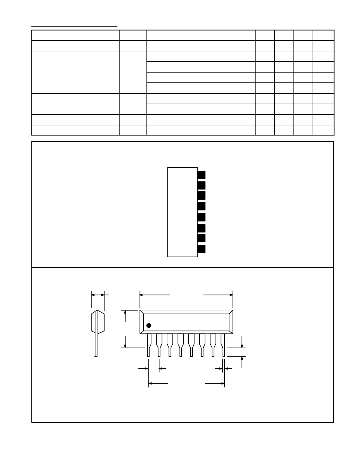
Pin Connection Diagram
(Front View)
V
8
CC
Bootstrap
7
Output
6
GND (For Output)
5
rms
.362
(9.2)
GND (For Input)
4
Feedback
3
Bypass
2
Input
1
.800 (20.3).142 (3.6)
18
.100 (2.54)
.020 (0.50).100 (2.54)
.700 (17.78)
 Loading...