

NTE NTE7099, NTE7098 Datasheet

NTE7098 & NTE7099
Integrated Circuit
Current Mode Pulse Width Modulator (PWM)
Control Circuit
Description:
The NTE7098 and NTE7099 are integrated circuits in 8–Lead DIP type packages that incorporate a
new precision temperature–controlled oscillator to minimize variations in frequency. An internal
toggle flip–flop, which blanks the output off every other clock cycle, limits the duty–cycle range to less
than 50%. An under–voltage lockout ensures that V
abled.
Other features include low start–up current, pulse–by–current limiting, and high–current totem pole
output for driving capacitive loads, such as the gate of a power MOSFET. The output is low in the
off state, consistent with N–channel devices.
Features:
D Optimized for Off–Line Control
D Temperature Compensated Oscillator
D 50% Maximum Duty–Cycle Clamp
D V
D Low Start–Up Current
D Pulse–by Pulse Current Limiting
D Improved U/V Lockout
D Double Pulse Suppression
D 1% Trimmed Bandgap Reference
D High Current Totem Pole Output
Stabilized before Output Stage is Enabled
ref
is stabilized before the output stage is en-
REF
Absolute Maximum Ratings:
Supply Voltage (ICC < 30mA) Self Limiting. . . . . . . . . . . . . . . . . . . . . . . . . . . . . . . . . . . . . . . . . . . . . . . . .
Supply Voltage (Low Impedence Source) 30V. . . . . . . . . . . . . . . . . . . . . . . . . . . . . . . . . . . . . . . . . . . . . .
Output Current ±1A. . . . . . . . . . . . . . . . . . . . . . . . . . . . . . . . . . . . . . . . . . . . . . . . . . . . . . . . . . . . . . . . . . . . .
Output Energy (Capacitive Load) 5µJ. . . . . . . . . . . . . . . . . . . . . . . . . . . . . . . . . . . . . . . . . . . . . . . . . . . . .
Analog Inputs (VFB, V
Error Amp Output Sink Current 10mA. . . . . . . . . . . . . . . . . . . . . . . . . . . . . . . . . . . . . . . . . . . . . . . . . . . . .
SENSE
) –0.3V to V
. . . . . . . . . . . . . . . . . . . . . . . . . . . . . . . . . . . . . . . . . . . . . . . . .
CC
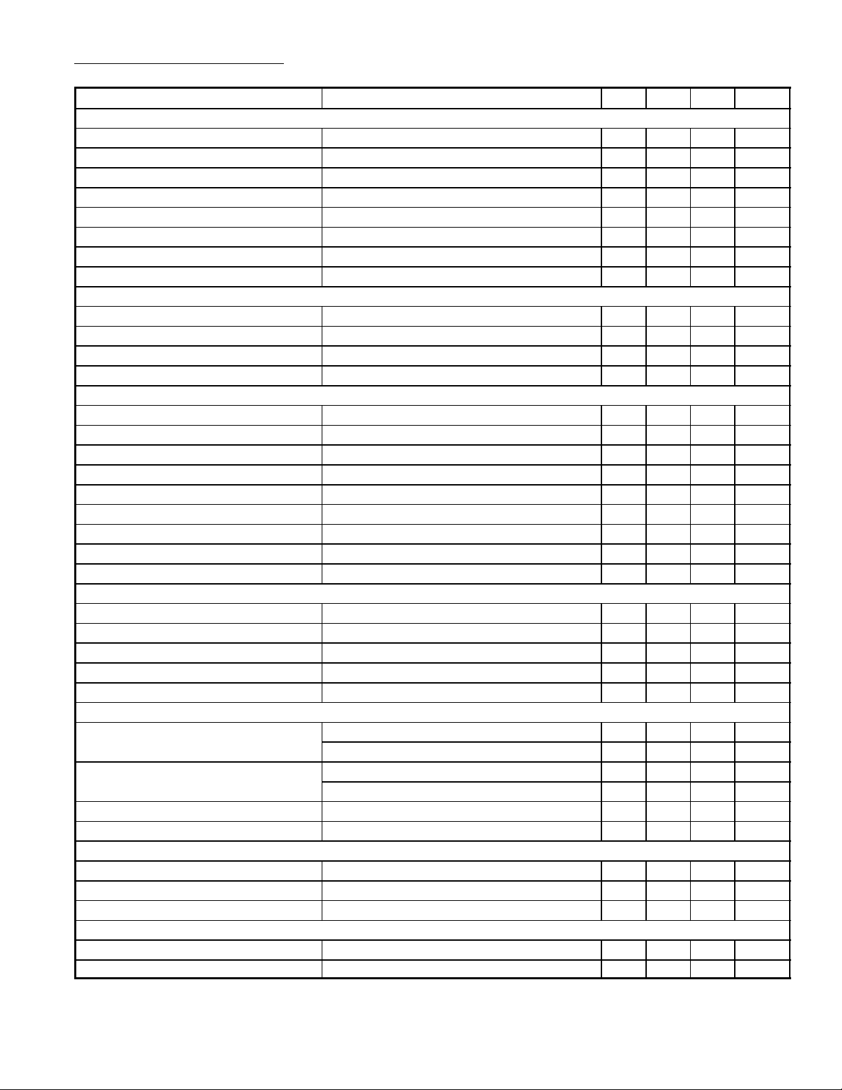
Elecrtrical Characteristics: (0° ≤ TA ≤ +70°C, VCC = 15V, RT = 10K, CT = 3.3nF for sawtooth
mode, Note 1 unless otherwise specified)
Parameter Test Conditions Min Typ Max Unit
Reference Section
Output Voltage TJ = +25°C, I
Line Regulation 12V ≤ VIN ≤ 25V – 6 20 mV
Load Regulation 1mA ≤ I
REF
Temperature Stability Note 2 – 0.2 0.4 mV/°C
Total Output Variation Line, Load, Temperature, Note 2 4.82 – 5.18 V
Output Noise Voltage 10Hz ≤ f ≤ 10kHz, TJ = +25°C, Note 2 – 50 – µV
Long Term Stability TA = +125°C, 1000Hrs., Note 2 – 5 25 mV
Output Short Circuit TA = +25°C –30 –100 –180 mA
Oscillator Section
Initial Accuracy Sawtooth Mode, TJ = +25°C 47 52 57 kHz
Voltage Stability 12V ≤ VCC ≤ 25V – 0.2 1.0 %
Temperature Stability Sawtooth Mode, 0° ≤ TA ≤ +70°C, Note 2 – 5 – %
Amplitude V
peak to peak – 1.7 – V
PIN4
Error Amp Section
Input Voltage V
= 2.5V 2.42 2.50 2.58 V
COMP
Input Bias Current VFB = 0V – –0.3 –2.0 µA
A
VOL
2V ≤ VO ≤ 4V 65 90 – dB
Unity Gain Bandwidth Note 2 0.7 1.0 – MHz
PSRR 12V ≤ VCC ≤ 25V 60 70 – dB
Output Sink Current VFB = 2.7V, V
Output Source Current VFB = 2.3V, V
V
High VFB = 2.3V, RL = 15K to GND 5 6 – V
OUT
V
Low VFB = 2.7V, RL = 15K to Pin8 – 0.7 1.1 V
OUT
Current Sense Section
Gain Note 3, Note 4 2.85 3.00 3.15 V/V
Maximum Input Signal V
= 5V, Note 3 0.9 1.0 1.1 V
COMP
PSRR 12V ≤ VCC ≤ 25V, Note 3 – 70 – dB
Input Bias Current V
= 0V – –2 –10 µA
SENSE
Delay to Output TJ = +25°C, Note 2 – 150 300 ns
Output Section
Output Low Level I
Output High Level I
= 20mA – 0.1 0.4 V
SINK
I
= 200mA – 1.5 2.2 V
SINK
SOURCE
I
SOURCE
= 20mA 13.0 13.5 – V
= 200mA 12.0 13.5 – V
Rise Time TJ = +25°C,CL = 1nF, Note 2 – 50 150 ns
Fall Time TJ = +25°C,CL = 1nF, Note 2 – 50 150 ns
Total Standby Current
Start–Up Current – 0.5 1.0 mA
Operating Supply Current VFB = V
SENSE
VCC Zener Voltage ICC = 25mA – 34 – V
PWM Section
Maximum Duty Cycle 46 48 50 %
Minimum Duty Cycle – – 0 %
= 1mA 4.9 5.0 5.1 V
REF
≤ 20mA – 6 25 mV
= 1.1V 2 6 – mA
COMP
= 5V –0.5 –0.8 – mA
COMP
= 0V, RT = 10K, CT = 3.3nF – 11 17 mA
 Loading...