

NTE NTE7088 Datasheet
NTE7088
Integrated Circuit
Audio Power Amplifier,
18 Watt BTL x 2 Channel
Description:
The NTE7088 is an integrated circuit in a 17–Lead Staggered SIP type package designed for car audio applications. This device has two built–in channels to reduce the characteristic difference betwee
Left and Right channels. In addition, the functions of stand–by and muting, and a variety of protection
circuits are included.
Features:
D Low Thermal Resistance
D High Power
D Low Distortion Ratio
D Low Noise
D Built–In Stand–by Function
D Built–In Muting Function
D Built–In Protection Circuits:
Thermal Shutdown, Overvoltage, Out → VCC short, Out → GND short, OUT – OUT short
Absolute Maximum Ratings: (TA = +25°C unless otherwise specified)
Peak Supply Voltage (0.2sec), VCC surge 50V. . . . . . . . . . . . . . . . . . . . . . . . . . . . . . . . . . . . . . . . . . . . .
DC Supply Voltage, VCC DC 25V. . . . . . . . . . . . . . . . . . . . . . . . . . . . . . . . . . . . . . . . . . . . . . . . . . . . . . . . .
Operating Supply Voltage, VCC opr 18V. . . . . . . . . . . . . . . . . . . . . . . . . . . . . . . . . . . . . . . . . . . . . . . . . . .
Output Current (Peak), IO (peak) 9A. . . . . . . . . . . . . . . . . . . . . . . . . . . . . . . . . . . . . . . . . . . . . . . . . . . . . .
Power Dissipation, P
D
Operating Temperature Range, T
Storage Temperature Range, T
stg
opr
–30° to +85°C. . . . . . . . . . . . . . . . . . . . . . . . . . . . . . . . . . . . . . . . .
–55° to +150°C. . . . . . . . . . . . . . . . . . . . . . . . . . . . . . . . . . . . . . . . . .
50W. . . . . . . . . . . . . . . . . . . . . . . . . . . . . . . . . . . . . . . . . . . . . . . . . . . . . . . . . . . . .
Electrical Characteristics: (VCC = 13.2V, RL = 4Ω, f = 1kHz, TA = +25°C unless otherwise specified)
Parameter Symbol Test Conditions Min Typ Max Unit
Quiescent Supply Current I
Output Power P
P
CCQ
OUT(1)
OUT(2)
VIN = 0 – 120 250 mA
VCC = 14.4V, THD = 10% – 18 – W
THD = 10% 11 15 – W
Electrical Characteristics (Cont’d): (VCC = 13.2V, RL = 4Ω, f = 1kHz, TA = +25°C unless otherwise
specified)
Parameter Symbol Test Conditions Min Typ Max Unit
Total Harmonic Distortion Ratio THD P
Voltage Gain G
Output Noise Voltage V
Ripple Rejection Ratio RR f
Input Resistance R
Output Offset Voltage V
Current at Stand–by State I
Crosstalk CT Rg = 600Ω, V
Pin4 Control Voltage V (SB) Stand–by → OFF (Power → ON) 2.5 – V
Pin1 Control Voltage V (MUTE) Mute → ON (Power → OFF) – 1.0 2.0 V
V
NO
IN
offset
SB
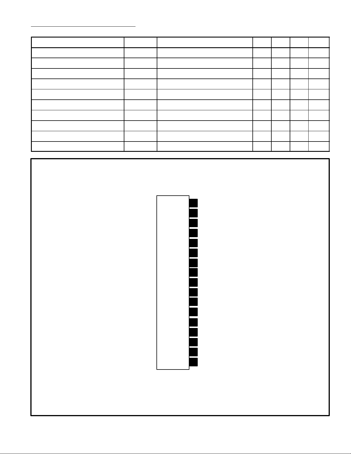
Pin Connection Diagram
= 1W – 0.04 0.4 %
OUT
48 50 52 dB
Rg = 0Ω, BW = 20Hz to 20kHz – 0.3 0.7 nV
= 100Hz, Rg = 600Ω 40 54 – dB
ripple
– 30 – kΩ
VIN = 0 –0.3 0 +0.3 V
– 1 10 µA
= 0dBm – 60 – dB
OUT
CC
(Front View)
17
Power VCC2
Output 2
16
rms
V
Output 1
15
GND 1
14
GND 2
13
Output 4
12
Output 3
11
Power VCC1
10
Pre–V
9
8
Ripple
CC
7 Input 2
6 NF 2
Pre–GND
5
Stand–By Switch
4
NF 1
3
Input 12
Mute Switch
1
 Loading...