

NTE NTE7085 Datasheet
NTE7085
Integrated Circuit
Vertical Deflection Output Circuit
w
/Drive Circuit for Monitor
Description:
The NTE7085 is an integrated circuit in a 13–Lead SIP type package that contains a vertical deflection
output circuit with a driver for color, B/W TV sets, monitors, and display units with a large aperture
(maximum current 2.2A
The NTE7085 can be used in conjunction with the NTE1863 (NTSC) to provide all the functions required for color TV signal processing.
Features:
D Low Power Dissipation due to On–Chip Pump–Up Circuit
D On–Chip 50/60Hz Vertical Size Control Circuit
D On–Chip Ramp Generator
D On–Chip Driver Circuit
D Vertical Output Circuit
D On–Chip Thermal Protection Circuit
D Minimum Number of External Parts Required
P–P
).
Absolute Maximum Ratings: (TA = +25°C unless otherwise specified)
Driver Circuit Supply Voltage, +VCC1max 15V. . . . . . . . . . . . . . . . . . . . . . . . . . . . . . . . . . . . . . . . . . . . . .
Pump–Up Circuit Supply Voltage, +VCC7max 30V. . . . . . . . . . . . . . . . . . . . . . . . . . . . . . . . . . . . . . . . . .
Output Circuit Supply Voltage, +VCC12max 62V. . . . . . . . . . . . . . . . . . . . . . . . . . . . . . . . . . . . . . . . . . . .
Deflection Output Current, I
. . . . . . . . . . . . . . . . . . . . . . . . . . . . . . . . . . . . . . . . . .
DEF
–1.5 to +1.5A
Allowable Power Dissipation (With Infinite Heat Sink), Pdmax 8W. . . . . . . . . . . . . . . . . . . . . . . . . . . .
Operating Temperature Range, T
Storage Temperature Range, T
opr
stg
Thermal Resistance, Junction–to–Case, R
thJC
–20° to +85°C. . . . . . . . . . . . . . . . . . . . . . . . . . . . . . . . . . . . . . . . .
–40° to +150°C. . . . . . . . . . . . . . . . . . . . . . . . . . . . . . . . . . . . . . . . . .
+4°C/W. . . . . . . . . . . . . . . . . . . . . . . . . . . . . . . . . . . . .
Operating Supply Voltage Conditions:
Driver Circuit Supply Voltage, +VCC1 8 to 14V. . . . . . . . . . . . . . . . . . . . . . . . . . . . . . . . . . . . . . . . . . . . .
Pump–Up Circuit Supply Voltage, +VCC7 10 to 27V. . . . . . . . . . . . . . . . . . . . . . . . . . . . . . . . . . . . . . . . .
Recommended Operating Conditions:
Driver Circuit Supply Voltage, +VCC1 12V. . . . . . . . . . . . . . . . . . . . . . . . . . . . . . . . . . . . . . . . . . . . . . . . .
Pump–Up Circuit Supply Voltage, +VCC7 24V. . . . . . . . . . . . . . . . . . . . . . . . . . . . . . . . . . . . . . . . . . . . . .
Maximum Deflection Output Current, I
11P–P
. . . . . . . . . . . . . . . . . . . . . . . . . . . . . . . . . . . . . . . .
2.2A
P–O
P–P
Electrical Characteristics: (TA = +25°C, +VCC1 = 12V, +VCC7 = 24V unless otherwise specified)
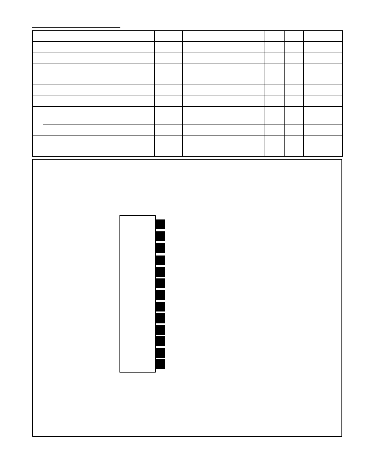
Parameter Symbol Test Conditions Min Typ Max Unit
Quiescent Current in Driver Power Supply I
Trigger Input Threshold Voltage V
Voltage on Vertical Size Control Pin V
Ramp Waveform Shape Start Voltage V
Pump–Up Charge Saturation Voltage V
Pump–Up Discharge Saturation Voltage V
Deflection Output Saturation Voltage
Lower
Upper V
Idling Current 16 22 32 mA
Voltage gain G
CC1
2
3
RAMP
S8–10
S8–10
V
S11–10
S12–11
Pin Connection Diagram
I = 1.1A – – 3.2 V
I = 1.1A – – 1.5 V
I = 1.1A – – 3.5 V
f = 1kHz – 59 – dB
VO
(Front View)
1.8 2.8 3.8 mA
2.8 3.1 3.4 V
5.9 6.1 6.3 V
4.7 5.0 5.3 V
– – 1.5 V
Ripple Filter
13
12
Power Supply for Vertical Output
Vertical Output
11
GND
10
OSC Blocking
9
Pump–Up Output
8
7
VCC7
6
AC/DC Feedback Input to Vertical Output Section
5
Ramp Waveform Generator
4
50/60Hz Vertical Size Control Signal Input
Vertical Height Control
3
V ertical Trigger Input
2
1
VCC1
 Loading...