

NTE NTE7083 Datasheet
NTE7083
Integrated Circuit
Vertical Deflection Circuit for
Monitor Applications
Description:
The NTE7083 is an integrated circuit in a 13–Lead Staggered SIP type package designed for vertical
deflection primarily in monitors and TV receivers.
Features:
D Fully Integrated, Few External Components
D RC Oscillator with Wide Sync Range
D Guard Circuit for Screen Protection
D Synchronization by Positive or Negative
Going Sync Pulse
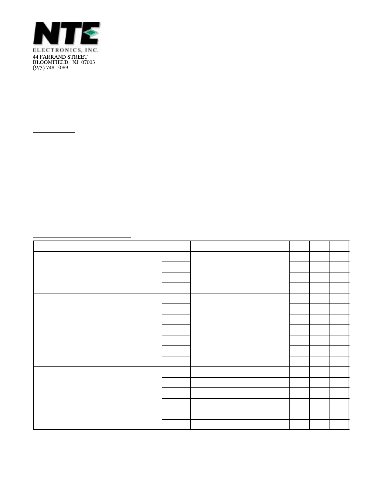
Absolute Maximum Ratings:
Parameter Symbol Test Conditions Min Max Unit
D Preamplifier
D Flyback Generator
D Internal Voltage Stabilizer
D Dual Frequency Criterion for Automatic
Amplitude Switch–Over
Voltages V
V
V
V
Supply Voltages (VP) V
Currents I
I6, I7, I8Note 1
2
11
12
13
10
V
9
V
7
V
6
V
5
V
4
V
3
1
I
3
I
4
I
9
I
11
0 6 V
0 24 V
0 6 V
0 50 V
0 50 V
0 50 V
0 60 V
0 60 V
0 6 V
0 24 V
–0.7 6 V
0 –1 mA
+3 –10 mA
0 –5 mA
–1.5 +1.5 A
–0.1 +3.0 mA
Note 1. I6, I7, and I8 are limited by SOAR protection circuit that ensures that a short–circuit between
the output Pin7 and supply voltage or GND does not destroy the output stage. A short circuit
may be soldered into the printed circuit board or may sometimes (non–periodically) occur
in the applied circuit.
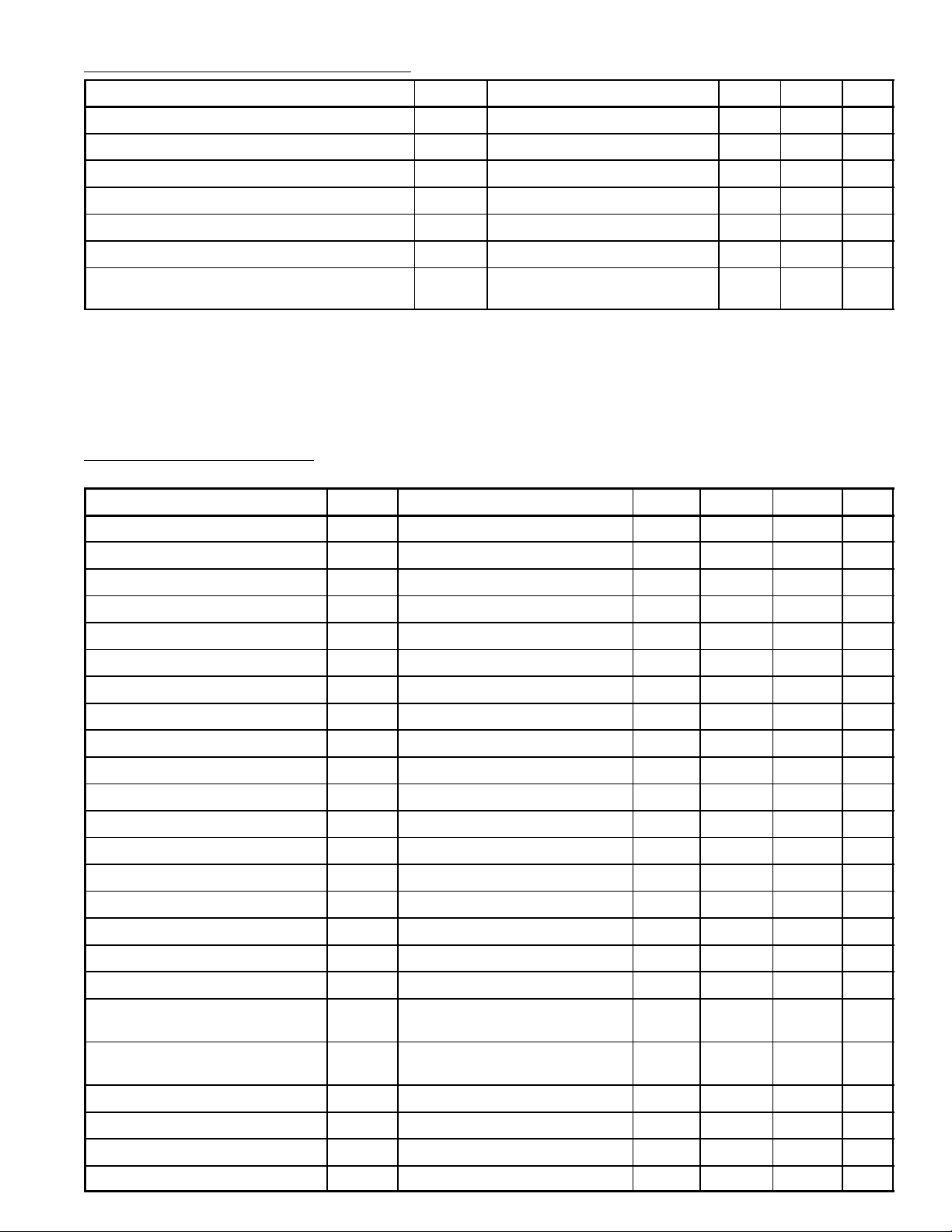
Absolute Maximum Ratings (Cont’d):
Parameter Symbol Test Conditions Min Max Unit
Storage Temperature Range T
Operating Ambient Temperature Range T
stg
Note 2 –20 +70 °C
A
–25 +150 °C
Maximum Junction Temperature TJmax Note 3 – +150 °C
Total Power Dissipation P
ESO Stability V
Thermal Resistance, Junction–to–Ambient R
Thermal Resistance, Junction–to–Mounting
R
ESO
thJA
thJMB
Note 2 – – W
tot
Note 4 –2000 +2000 V
– 20 K/W
– 5 K/W
Base
Note 2. The maximum value to the operating ambient temperature range and the power dissipation
depends on the heatsink.
Note 3. Internally liminted by thermal protection: switching temperature point at TJ = +150°C ±8°C.
Note 4. Human body model: 1.5kΩ, 100pF, 5 pulses.
Electrical Characteristics: (All voltages are measured to V
(Pin8), TA = +25°C, VP = +23V
GND
unless otherwise specified)
Parameter Symbol Test Conditions Min Typ Max Unit
Supply Voltage Range (Pin10) V
Supply Voltage Range (Pin6) V
Supply Current I
Supply Current I
Supply Current I
Minimum Output Voltage V
Maximum Output Voltage V
Output Voltage During Flyback V
Output Current I
Output Current I
Preamplifier Input Current I
Stabilized Voltage V
Blanking Pulse Output Voltage V
Blanking Pulse Output Resistance R
Blanking Pulse Output Current I
Blanking Pulse Duration t
Output Voltage Ramp Generator V
Output Current Ramp Generator I
Output Voltage Frequency Detec-
V
tor
P
P
V10 = 25V, V5 = 3V without load – 12 – mA
10
V6 = 25V, V5 = 1V without load – 20 – mA
6
V6 = 25V, V5 = 3V withput load – 5 – mA
6
I7 = 1A – 1.40 1.65 V
7
I7 = 1A V6 –2.3 V6 –2.0 – V
7
I9 = –1A – V10 –2.2 – V
9
7
8
5
1
3
3
3
R = 100Ω, C = 10pF (Pin12) 640 680 730 µs
bl
11
11
Lower Frequency I13 = 1mA – – 1.0 V
13
10 – 45 V
10 – 30 V
– – ±1.3 A
– – ±1.3 A
– –0.1 – µA
6.1 6.8 7.3 V
– 5.7 – V
– 300 – Ω
0 – –3 mA
0.3 – 20 V
–2 – 15 x 1 03µA
Leakage Current Frequency
Detector
Output Voltage Buffer Stage V
Output Current Buffer Stage I
Synchronizing Input Voltage V
Synchronizing Input Voltage V
I
Higher Frequency V13 = 50V – – 1.0 µA
13
4
4
Positive Sync 1.0 – 6.0 V
3
Negative Sync –0.5 – –0.7 V
3
0 – 20 V
– – –4.0 mA
 Loading...