

NTE NTE7081 Datasheet

NTE7081
Integrated Circuit
RGB Video Amplifier System
Description:
The NTE7081 is a wideband video amplifier system in a 28–Lead DIP type package intended for high
resolution RGB color monitor applications. In addition to three matched video amplifiers, the
NTE7081 contains three gated differential input black level clamp comparators for brightness control
and three matched attenuator circuits for contrast control. Each video amplifier contains a gain set
or “Drive” node for setting maximum system gain (AV = 4 to 10) as well as providing trim capability.
The NTE7081 also contains a voltage reference for the video inputs.
Features:
D Three Wideband Video Amplifiers (70MHz @ –3dB)
D Inherently Matched (±0.5dB) Attenuators for Contrast Control
D Three Externally Gated Comparators for Brightness Control
D Provisions for Independent Gain Control (Drive) of each Video Amplifier
D Video Input Voltage Reference
D Low Impedance Output Driver
Absolute Maximum Ratings:
Supply Voltage (Pin1, Pin13, Pin23, Pin28, Note 1), V
Voltage at Any Input Pin, V
Video Output Current, I16, I20, or I
Power Dissipation (Note 2), P
IN
28
D
CC
VCC ≥ VIN ≥ GND. . . . . . . . . . . . . . . . . . . . . . . . . . . . . . . . . . . . . . . . . . . . .
13.5V. . . . . . . . . . . . . . . . . . . . . . . . . . . . . .
28mA. . . . . . . . . . . . . . . . . . . . . . . . . . . . . . . . . . . . . . . . . . . . . . . .
2.5W. . . . . . . . . . . . . . . . . . . . . . . . . . . . . . . . . . . . . . . . . . . . . . . . . . . . . .
Junction Temperature, TJ +150°C. . . . . . . . . . . . . . . . . . . . . . . . . . . . . . . . . . . . . . . . . . . . . . . . . . . . . . . .
Operating Temperature Range, TA 0° to +70°C. . . . . . . . . . . . . . . . . . . . . . . . . . . . . . . . . . . . . . . . . . . .
Storage Temperature Range, T
Thermal Resistance, Junction–to–Ambient, R
Lead Temperature (During Soldering, 10sec.) , T
–65° to +150°C. . . . . . . . . . . . . . . . . . . . . . . . . . . . . . . . . . . . . . . . . .
stg
thJA
L
50°C/W. . . . . . . . . . . . . . . . . . . . . . . . . . . . . . . . . . . .
+265°C. . . . . . . . . . . . . . . . . . . . . . . . . . . . . . . . . . .
ESD susceptibility 2kV. . . . . . . . . . . . . . . . . . . . . . . . . . . . . . . . . . . . . . . . . . . . . . . . . . . . . . . . . . . . . . . . .
Note 1. VCC s uppl y pins 1 , 1 3, 2 3, a nd 2 8 m ust b e e xternal ly wired t ogether t o p revent i nternal d amage
during VCC power ON/OFF cycles.
Note 2. Derate above +25°C based on R
thJA
and TJ.
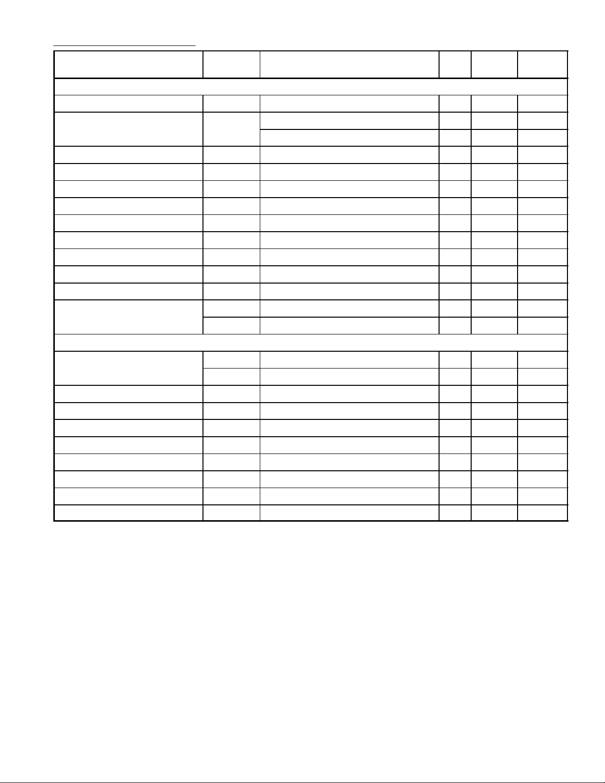
Electrical Characteristics: (TA = +25°C, V
CC1
= V
= 12V unless otherwise specified)
CC2
Parameter Symbol Test Conditions Typ
DC Static Test (S17, S21, S26 Open, V12 = 6V, V14 = 0V, V15 = 2V unless otherwise specified)
Tested
(Note 3)
(Limits)
Unit
Supply Current I
Video Input Reference Voltage V
Video Input Bias Current I
Clamp Gate Low Input Voltage V
Clamp Gate High Input Voltage V
Clamp Gate Low Input Current I
Clamp Gate High Input Current I
Clamp Cap Charge Current I
Clamp Cap Discharge Current I
clamp(+)
clamp(–)
Video Output Low Voltage V
Video Output High Voltage V
S
11
b
14L
14H
14L
14H
OL
OH
VCC1 Only 73 90 mA Max
2.4 2.2 V
– 2.6 V
MIN
MAX
Any One Amplifier 5 20 µA Max
Clamp Comparators ON 1.2 0.8 V
Clamp Comparators OFF 1.6 2.0 V
MIN
MAX
V14 = 0V –0.5 –5.0 µA Max
V14 = V
CC
0.005 1.0 µA Max
V5, V8, or V10 = 0V 850 – µA
V5, V8, or V10 = 5V –850 – µA
V5, V8, or V10 = 0V 1.2 – V
V5, V8, or V10 = 5V 8.9 – V
Video Output Offset Voltage ∆VO(2V) Between Any Two Amplifiers, V15 = 2V ±0.5 ±50 mV Max
∆VO(4V) Between Any Two Amplifiers, V15 = 4V ±0.5 ±50 mV Max
AC Dymanic Test (S17, S21, S26 Closed, V14 = 0V, V15 = 4V, f = 10kHz unless otherwise specified)
Video Amplifier Gain AVmax V12 = 12V, VIN = 560mV
AVmid V12 = 5V, VIN = 560mV
V12 for AV Low V12low VIN = 1V
, Note 4 2.0 – V
P–P
P–P
P–P
6.6 – V/V
2.0 – V/V
Video Gain Match at AVmax ∆AVmax V12 = 12V, Note 5 ±0.2 – dB
Video Gain Match at AVmid ∆AVmid V12 = 5V, Note 5 ±0.2 – dB
Video Gain Match at AVlow ∆AVlow V12 = V12low, Note 4, Note 5 ±0.3 – dB
Video Amplifier Distortion THD V12 = 3V, VIN = 1V
P–P
0.5 – %
Video Amplifier Bandwidth f (–3dB) V12 = 12V, Note 6, Note 8 70 – MHz
Video Amplifier, 10kHz Isolation V
Video Amplifier, 10MHz Isolation V
10kHz V12 = 12V, Note 7 –60 – dB
sep
10MHz V12 = 12V, Note 7, Note 8 –40 – dB
sep
Note 3. These parameters are guaranteed and 100% tested.
Note 4. Determine V12 low for –40dB attenuation of output. Reference AV to max.
Note 5. Measure gain difference between any two amplifiers. VIN = 1V
P–P
.
Note 6. Adjust input frequency, fIN, from 10kHz (AV max ref level) to the –3dB corner frequency
(f –3dB). VIN = 560mV
Note 7. VIN = 560mV
at fIN = 10kHz to any one amplifier . Measure output levels of the other two
P–P
P–P
.
undriven amplifiers relative to driven amplifier to determine channel separation. Terminate
the undriven amplifier inputs to simulate generator loading. Repeat test at fIN = 10MHz for
V
= 10MHz.
sep
Note 8. Special test fixture without socket required.
 Loading...