

NTE NTE708 Datasheet
NTE708
Integrated Circuit
TV/FM Sound IF Amplifier
Features:
D Greatly Simplifier FM Demodulator Alignment
D Excellent Performance at V+ = 8V
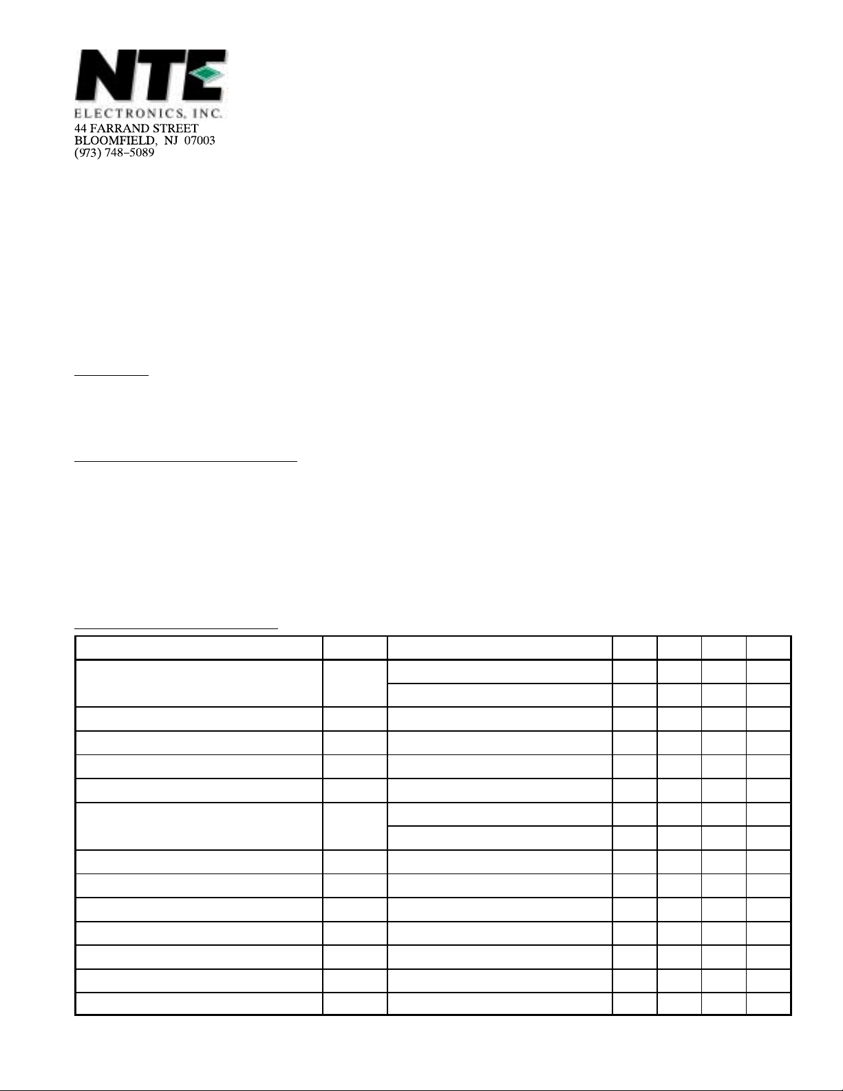
Absolute Maximum Ratings:
(TA = +25°C unless otherwise specified)
Power Supply Voltage 16V. . . . . . . . . . . . . . . . . . . . . . . . . . . . . . . . . . . . . . . . . . . . . . . . . . . . . . . . . . . . . .
Peak Input Voltage (Pin4) 3.5V. . . . . . . . . . . . . . . . . . . . . . . . . . . . . . . . . . . . . . . . . . . . . . . . . . . . . . . . . .
Power Dissipation (T
= +25°C), P
A
D
625mW. . . . . . . . . . . . . . . . . . . . . . . . . . . . . . . . . . . . . . . . . . . . . .
Derate Above 25°C 5mW/°C. . . . . . . . . . . . . . . . . . . . . . . . . . . . . . . . . . . . . . . . . . . . . . . . . . . . . . .
Operating Ambient Temperature Range, T
Storage Temperature Range, T
Electrical Characteristics:
Parameter Pin Test Conditions Min Typ Max Unit
Drain Current 13 V+ = 8V 10 12 19 mA
Amplifier Input Reference Voltage 6 – 1.45 – V
Detector Input Reference Voltage 2 – 3.65 – V
Amplifier High Level Output Voltage 10 1.25 1.45 1.65 V
Amplifier Low Level Output Voltage 9 – 0.145 0.2 V
Detector Output Voltage 1 V+ = 8V – 3.7 – V
stg
(V+ = 12V, TA = +25°C unless otherwise specified)
opr
V+ = 12V – 15 21 mA
V+ = 12V – 5.4 – V
0° to +75°C. . . . . . . . . . . . . . . . . . . . . . . . . . . . . . . . . . . .
–65° to +150°C. . . . . . . . . . . . . . . . . . . . . . . . . . . . . . . . . . . . . . . . . .
Amplifier Input Resistance 4 – 5.0 – kΩ
Amplifier Input Capacitance 4 – 11 – pF
Detector Input Resistance 12 – 70 – kΩ
Detector Input Capaciance 12 – 2.7 – pF
Amplifier Output Resistance 10 – 60 – Ω
Detector Output Resistance 1 – 200 – Ω
De–Emphasis Resistance 14 – 8.8 – kΩ
Dynamic Characteristics: (FM Modulation Freq = 1kHz, Source Resistance = 50Ω,
T
= +25°C for all tests)
A
Parameter Pin Test Conditions Min Typ Max Unit
(V+ = 12V, fo = 4.5MHz, ∆f = ±25kHz, Peak Separation = 150kHz)
Amplifier Voltage Gain 10 Vin ≤ 50µV
AM Rejection 1 Vin = 10mV
rms
, Note 1 – 36 – dB
rms
– 60 – dB
Input Limiting Threshold Voltage 4 – 250 – µV
Recovered Audio Output Voltage 1 Vin = 10mV
Output Distortion 1 Vin = 10mV
rms
rms
– 0.72 – V
– 3 – %
(V+ = 12V, fo = 5.5MHz, ∆f = ±50kHz, Peak Separation = 260kHz)
Amplifier Voltage Gain 10 Vin ≤ 50µV
AM Rejection 1 Vin = 10mV
rms
, Note 1 – 40 – dB
rms
– 60 – dB
Input Limiting Threshold Voltage 4 – 250 – µV
Recovered Audio Output Voltage 1 Vin = 10mV
Output Distortion 1 Vin = 10mV
rms
rms
– 1.2 – V
– 5 – %
(V+ = 8V, fo = 10.7MHz, ∆f = ±75kHz, Peak Separation = 550kHz)
Amplifier Voltage Gain 10 Vin ≤ 50µV
AM Rejection 1 Vin = 10mV
rms
, Note 1 – 37 – dB
rms
– 53 – dB
Input Limiting Threshold Voltage 4 – 600 – µV
Recovered Audio Output Voltage 1 Vin = 10mV
Output Distortion 1 Vin = 10mV
rms
rms
– 0.3 – V
– 1.4 – %
(V+ = 12V, fo = 10.7MHz, ∆f = ±75kHz, Peak Separation = 550kHz)
rms
rms
rms
rms
rms
rms
Amplifier Voltage Gain 10 Vin ≤ 50µV
AM Rejection 1 Vin = 10mV
rms
, Note 1 – 45 – dB
rms
– 53 – dB
Input Limiting Threshold Voltage 4 – 600 – µV
Recovered Audio Output Voltage 1 Vin = 10mV
Output Distortion 1 Vin = 10mV
rms
rms
– 0.48 – V
– 1.4 – %
Note 1. 100% FM, 30% AM Modulation.
Pin Connection Diagram
Audio Output
Detector Input Ref
N.C.
IF Input
1
2
3
4
5Decoupling
6IF Input Ref
7GND
14
De–Emphasis
V
13
CC
12
Det Input (QuadratureNetwork)
11
Test Point
10 Amplifier Output
9 Amplifier Low Output
8 N.C.
rms
rms
 Loading...