

NTE NTE7073 Datasheet
NTE7073
Integrated Circuit
Hybrid Switching Regulator
Absolute Maximum Ratings: (TA = +25°C unless otherwise specified)
TR1 Collector–Emitter Voltage (Note 1), V
Applying Voltage, Pin4–2, V
Applying Voltage, Pin2–5, V
Applying Voltage, Pin5–9, V
Applying Voltage, Pin7–6, V
TR1 Collector Current, I
2–4
2–5
5–9
7–6
C(TR1)
Continuous 10A. . . . . . . . . . . . . . . . . . . . . . . . . . . . . . . . . . . . . . . . . . . . . . . . . . . . . . . . . . . . . . . . . .
Pulsed 20A. . . . . . . . . . . . . . . . . . . . . . . . . . . . . . . . . . . . . . . . . . . . . . . . . . . . . . . . . . . . . . . . . . . . . .
TR4 Collector Current, I
D2 Forward Current, I
D3 Forward Current, I
C(TR4)
IN(D2)
IN(D3)
Maximum Power Dissipation (Note 2), P
No Fin 3.2W. . . . . . . . . . . . . . . . . . . . . . . . . . . . . . . . . . . . . . . . . . . . . . . . . . . . . . . . . . . . . . . . . . . . .
TC1 = +100°C 2.7W. . . . . . . . . . . . . . . . . . . . . . . . . . . . . . . . . . . . . . . . . . . . . . . . . . . . . . . . . . . . . . .
TR1 Junction Temperature, T
J
Frame Temperature Range (Operating, Note 3), T
Storage Temperature Range, T
stg
Maximum Output Current (VO = 115V), I
CEX
D
C2
O
500V. . . . . . . . . . . . . . . . . . . . . . . . . . . . . . . . . . . . . . . . .
12V. . . . . . . . . . . . . . . . . . . . . . . . . . . . . . . . . . . . . . . . . . . . . . . . . . . . . . .
12V. . . . . . . . . . . . . . . . . . . . . . . . . . . . . . . . . . . . . . . . . . . . . . . . . . . . . . .
30V. . . . . . . . . . . . . . . . . . . . . . . . . . . . . . . . . . . . . . . . . . . . . . . . . . . . . . .
5V. . . . . . . . . . . . . . . . . . . . . . . . . . . . . . . . . . . . . . . . . . . . . . . . . . . . . . . .
500mA. . . . . . . . . . . . . . . . . . . . . . . . . . . . . . . . . . . . . . . . . . . . . . . . . . . . .
500mA. . . . . . . . . . . . . . . . . . . . . . . . . . . . . . . . . . . . . . . . . . . . . . . . . . . . . . .
100mA. . . . . . . . . . . . . . . . . . . . . . . . . . . . . . . . . . . . . . . . . . . . . . . . . . . . . . .
+150°C. . . . . . . . . . . . . . . . . . . . . . . . . . . . . . . . . . . . . . . . . . . . . . . . . . . .
–20° to +125°C. . . . . . . . . . . . . . . . . . . . . . . . . .
–30° to +125°C. . . . . . . . . . . . . . . . . . . . . . . . . . . . . . . . . . . . . . . . . .
1.7A. . . . . . . . . . . . . . . . . . . . . . . . . . . . . . . . . . . . . . . . . . . .
Note 1. Reference: V
= 400V Min
CEO
Note 2. TC1 denotes the temperature of resin beneath the Power Transistor.
Note 3. TC2 denotes the internal frame temperature. Recommended TC2 = +100°C.
Electrical Characteristics (TR1 Characteristics): (TA = +25°C unless otherwise specified)
Parameter Symbol Test Conditions Min Typ Max Unit
Saturation Voltage V
Collector Cutoff Current I
DC Current Gain h
Power Transistor Thermal
Resistance
Switching Time t
CE(sat)IC
V
BE(sat)IC
R
CBO
FE
Θ
JC2
s
t
f
= 8A, IB = 1.2A – – 0.5 V
= 6A, IB = 1.2A – – 1.5 V
VCE = 500V, VBE = 1.5V – – 1.8 mA
IC = 1A, VCE = 4V 15 – 40
Between Junction and Internal Frame – 0.7 – °C/W
– – 10.0 µs
– – 0.6 µs
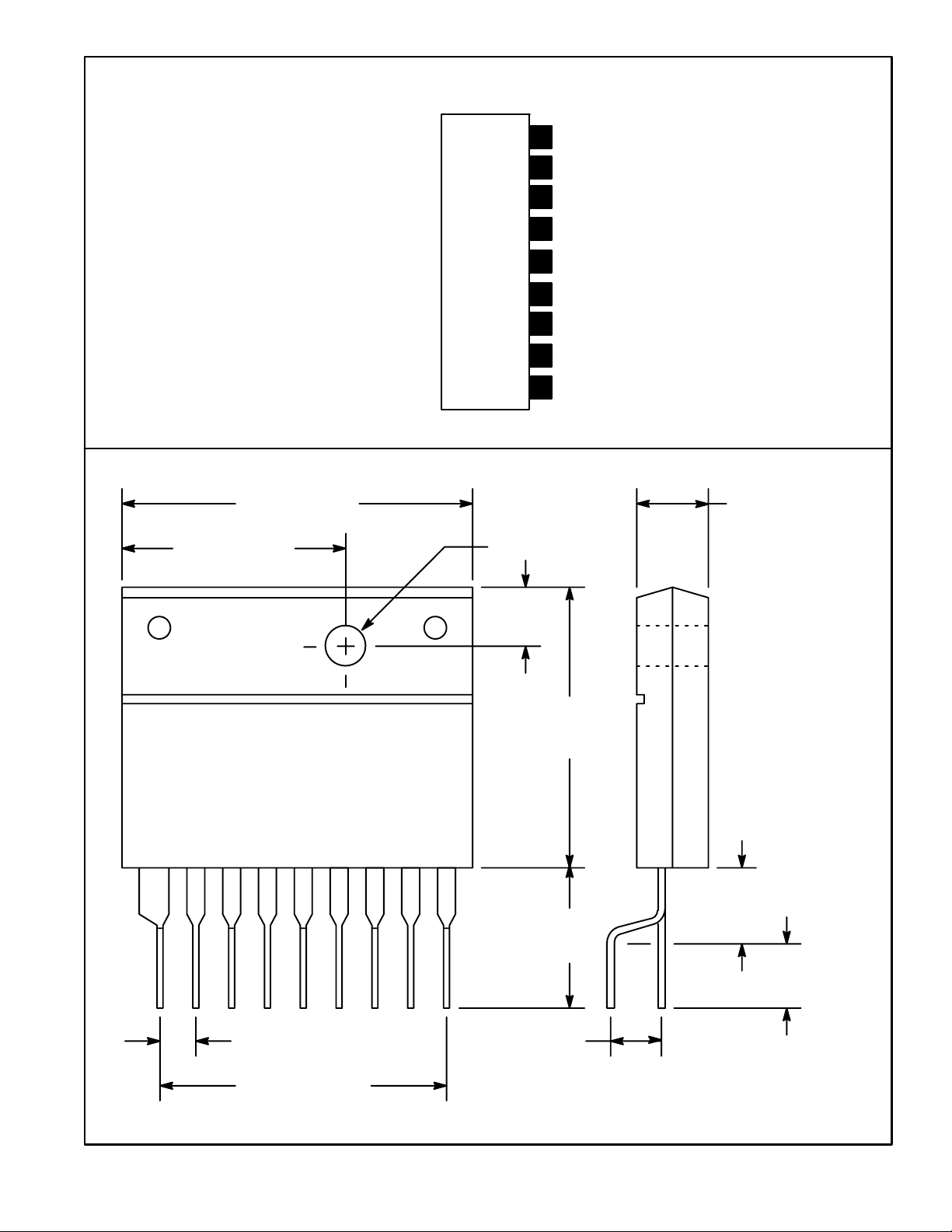
Pin Connection Diagram
(Front View)
Photo Coupler (–)
9
Drive TR2 Base
8
GND/Current Detector
7
Current Detector Base
6
5 Drive Control
4 Drive Control
Base
3
2
Emitter/Common (Power TR)
Collector1
.953 (24.4)
.610 (15.5)
.130 (3.3) Dia
.197
(5.0)
.905
(23.0)
19
.276
.492
(7.0)
(12.5)
.216 (5.5)
.100 (2.54) .177 (4.5)
.800 (20.32)
.216 (5.5)
 Loading...