

NTE NTE7072 Datasheet

NTE7072
Integrated Circuit
Dual DC Controlled Potentiometer Circuit
Description:
The NTE7072 is a monolithic integrated circuit designed for use as a volume and tone control circuit
in stereo amplifiers. This dual tandem potentiometer IC consists of two ganged pairs of electronic
potentiometers with eight inputs connected via impedance converters, and the four outputs driving
individual operational amplifiers. The setting of each electronic potentiometer pair is controlled by
an individual DC control voltage. The potentiometers operate by current division between the arms
of cross–coupled long–tailed pairs. The current division factor is determined by the level and polarity
of the DC control voltage with respect to an externally available reference level of half the supply voltage. Since the electronic potentiometers are adjusted by a DC control voltage, each pair can be controlled by single linear potentiometers which can be located in any position dictated by the equipment
styling. Since the input and feedback impedances around the operational amplifier gain blocks are
external, the NTE7072 can perform bass/treble and volume/loudness control. It also can be used as
a low–level fader to control the sound distribution between the front and rear loudspeakers in car radio
installations.
Features:
D High impedance inputs to both ‘ends’ of each electronic potentiometer
D Ganged potentiometers track within 0.5dB
D Electronic rejection of supply ripple
D Internally–generated reference level available externally so that the control voltage can be
made to swing positively and negatively around a well–defined 0V level
D The operational amplifiers have push–pull outputs for wide voltage swing and low current
consumption
D The operation amplifier outputs are current limited to provide output short–circuit protection
D Although designed to operate from a 20V supply (giving a maximum input and output signal level
of 6V), the NTE7072 can work from a supply as low as 7.5V with reduced input and output signal
levels
Applications:
D Volume Control
D Tone Control
D Low Level Fader
Absolute Maximum Ratings:
Supply Voltage (Pin11), V
CC
Control Voltages (Pin9 and Pin10) 1V. . . . . . . . . . . . . . . . . . . . . . . . . . . . . . . . . . . . . . . . . . . . . . . . . . . . .
Input Voltage Ranges at Pin3, Pin4, Pin5, Pin6, Pin13, Pin14, Pin15, and Pin16, V
(With respect to Pin18) 0 to V
Total Power Dissipation, P
Thermal Resistance, Crystal–to–Ambient, R
Operating Ambient Temperature Range, T
Storage Temperature Range, T
. . . . . . . . . . . . . . . . . . . . . . . . . . . . . . . . . . . . . . . . . . . . . . . . . . . .
TOT
thCRA
A
stg
I
800mW. . . . . . . . . . . . . . . . . . . . . . . . . . . . . . . . . . . . . . . . . . . . . . . . . . . . .
80°C/W. . . . . . . . . . . . . . . . . . . . . . . . . . . . . . . . . . .
–30° to +80°C. . . . . . . . . . . . . . . . . . . . . . . . . . . . . . . . . . .
–65° to +150°C. . . . . . . . . . . . . . . . . . . . . . . . . . . . . . . . . . . . . . . . . .
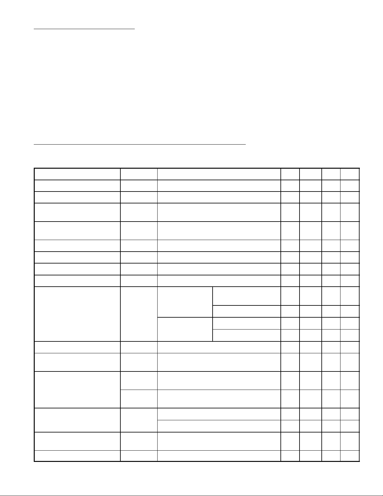
Electrical Characteristics (Treble and Bass Control Circuit): (TA = +25°C, VCC = 20V,
RG = 60Ω, RL > 4.7kΩ, CL < 30pF, f = 1kHz, with a linear frequency response
(VC1 = VC2 = 0V), unless otherwise specified)
Parameter Symbol Test Conditions Min Typ Max Unit
Supply Current I
Frequency Response (–1dB) f VC1 = VC2 = 0V 10 – 20k Hz
Voltage Gain A
CC
V
Without load 14 22 30 mA
at linear frequency response
(VC1 = VC2 = 0V)
– 0 – dB
23V. . . . . . . . . . . . . . . . . . . . . . . . . . . . . . . . . . . . . . . . . . . . . . . . . . . . . . . . .
CC
Gain Variation ∆A
Bass Boost at 40Hz (ref. 1kHz) VC2 = 120mV – 17.5 – dB
Bass Cut at 40Hz (ref. 1kHz) –VC2 = 120mV – 17.5 – dB
Treble Boost at 16kHz (ref. 1kHz) VC1 = 120mV – 16 – dB
Treble Cut at 16kHz (ref. 1kHz) –VC1 = 120mV – 16 – dB
Total Harmonic Distortion
Signal Level VI, V
Power Bandwidth BW at reference level V
Output Noise Voltage V
V
THD
O(RMS)
NO(RMS)
V
NO(M)
f = 1kHz, at maximum bass/treble boost or
cut at ±VC1 = ±VC2 = 120mV
V
V
THD = 0.7% (input and output) 5.5 6.2 – V
THD = 0.1%
signal plus noise (RMS) value,
f = 20Hz to 20kHz
noise (peak value) weighted to DIN 45405,
CCITT filter
= 300mV
O(RMS)
= 5V f = 1kHz – 0.015 0.1 %
O(RMS)
f = 1kHz
(measured selectively)
f = 20Hz to 20kHz – 0.005 – %
f = 20Hz to 20kHz – 0.05 0.1 %
= 5V (–3dB),
O(RMS)
– ±1 – dB
– 0.002 – %
– 40 – kHz
– 75 – µV
– 160 230 µV
Crosstalk Attenuation
(Stereo)
Control Voltage Crosstalk to
the Outputs
Ripple Rejection ∝100 f = 100Hz, V
∝CT f = 1kHz – 86 – dB
f = 20Hz to 20kHz – 80 – dB
–∝CT f = 1kHz, V
C1(RMS)
CC(RMS)
= V
C2(RMS)
< 200mV – 46 – dB
= 1mV – 20 – dB
 Loading...