

NTE NTE7052 Datasheet

NTE7052
Integrated Circuit
Mono BTL Audio Amplifier, 3W
Description:
The NTE7052 is a mono output amplifier in a 9–Lead SIP type package designed for use in battery–
fed portable radios and mains–fed equipment such as televisions. This device needs no external
components because it makes use of the Bridge–Tied–Load (BTL) principle. Consequently it has,
at the same supply voltage, a higher output power compared to a conventional Single Ended output
stages. The NTE7052 is capable of delivering an output power of 1W into a loudspeaker load of 8Ω
with a 6V supply or 3W into a 16Ω loudspeaker at 11V without the need of an external heatsink. The
gain is internally fixed at 40dB. Special attention is given to ON/OFF switch click suppression, and
it has a good overall stability. The load can be short circuited at all input conditions.
Features:
D No External Components
D No ON/OFF Switch Clicks
D Good Overall Stability
D Low Power Consumption
D Short–Circuit Protection
D ESD Protected on All Pins
Absolute Maximum Ratings:
Supply Voltage, V
Peak Repetitive Output Current, I
Peak Non–Repetitive Output Current, I
Total Power Dissipation (TC < +60°C), P
Short Circuit Time (Note 1), T
Junction Temperature, T
Storage Temperature Range, T
Thermal Resistance, Junction–to–Case, R
Thermal Resistance, Junction–to–Ambient, R
P
ORM
OSM
tot
SC
J
stg
thJC
thJA
Note 1. The load can be short–circuited at all input conditions.
18V. . . . . . . . . . . . . . . . . . . . . . . . . . . . . . . . . . . . . . . . . . . . . . . . . . . . . . . . . . . . . . . . .
1A. . . . . . . . . . . . . . . . . . . . . . . . . . . . . . . . . . . . . . . . . . . . . . . . . .
1.5A. . . . . . . . . . . . . . . . . . . . . . . . . . . . . . . . . . . . . . . . . . .
9W. . . . . . . . . . . . . . . . . . . . . . . . . . . . . . . . . . . . . . . . . . . . .
1Hr. . . . . . . . . . . . . . . . . . . . . . . . . . . . . . . . . . . . . . . . . . . . . . . . . . . . . .
+150°C. . . . . . . . . . . . . . . . . . . . . . . . . . . . . . . . . . . . . . . . . . . . . . . . . . . . . . . . .
–55° to +150°C. . . . . . . . . . . . . . . . . . . . . . . . . . . . . . . . . . . . . . . . . .
10K/W. . . . . . . . . . . . . . . . . . . . . . . . . . . . . . . . . . . . . .
55K/W. . . . . . . . . . . . . . . . . . . . . . . . . . . . . . . . . . . .
Electrical Characteristics: (TA = +25°C, VP = 11V, f = 1kHz, RL = 16Ω unless otherwise specified)
Parameter Symbol Test Conditions Min Typ Max Unit
Operating Supply Voltage V
Repetitive Peak Output Current I
ORM
Total Quiescent Current I
Output Power P
P
RL = ∞, Note 2 – 5 7 mA
P
THD = 10% 2.5 3.0 – W
O
3 11 18 V
– – 600 mA
Total Harmonic Distortion THD PO = 500mW – 0.25 1.0 %
Voltage Gain G
Noise Output Voltage V
V
Note 3 – 180 300 µV
no
39.0 40.5 42.0 dB
Note 4 – 60 – µV
Frequency Response 20 to 20,000 Hz
Ripple Rejection RR Note 5 36 50 – dB
DC Output Offset Voltage ∆V RS = 5kΩ – – 200 mV
Input Impedance |Zi| – 100 – kΩ
Input Bias Current I
I
– 100 300 nA
Note 2. With a load connected to the outputs the quiescent current will increase, the maximum value
of this increase being equal to the DC output offset voltage divided by RL.
Note 3. The noise output voltage (RMS value) is measured with RS = 5kΩ unweighted (20Hs to
20kHz).
Note 4. The n o ise o utput v olta ge (R MS v alue) a t f = 5 00 kHz i s m easur ed wi th RS = 0Ω and BW = 5kHz.
With a practical load (RL = 16Ω, LL = 200µH) the noise output current is only 50nA.
Note 5. The ripple rejection is measured with RS = 0Ω and f = 100Hz to 10kHz. The ripple voltage
(200mV) is applied to the positive supply rail.
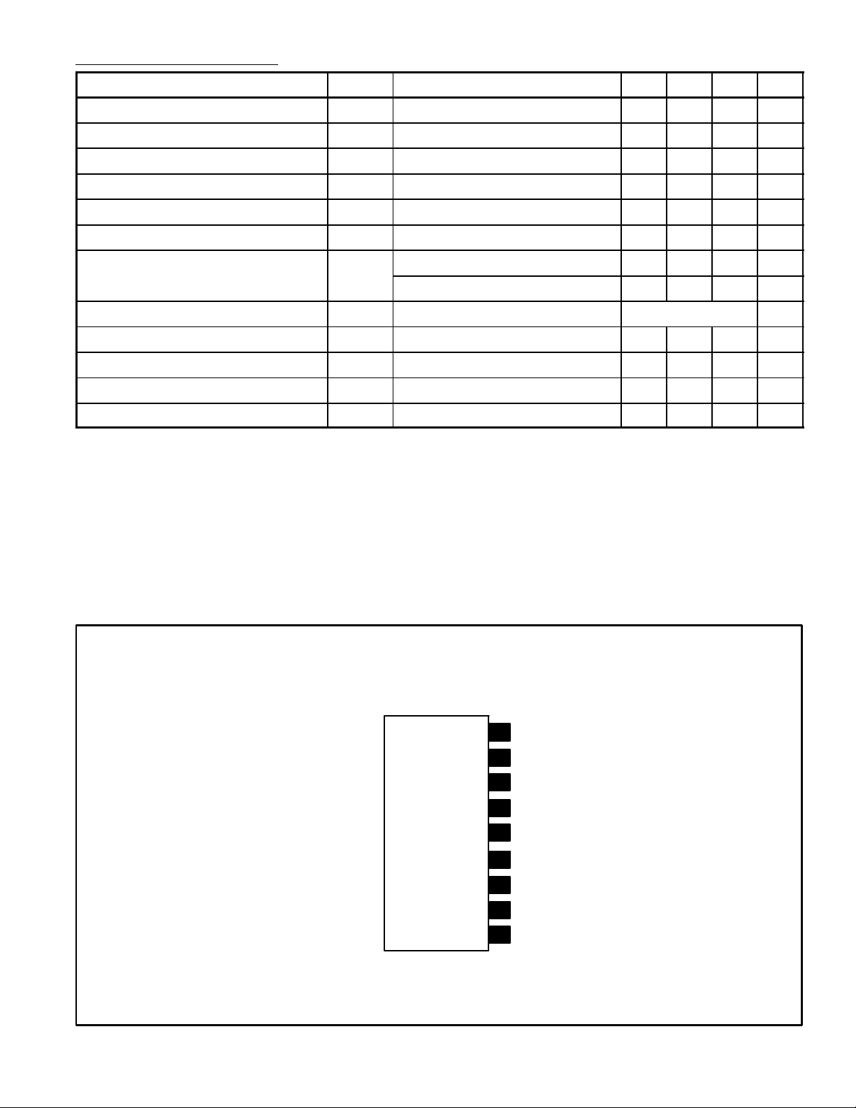
Pin Connection Diagram
(Front View)
N.C.
9
8
Output (–)
7
Power GND
Output (+)
6
5 N.C.
Signal GND
4
Input (+)
3
V
2
P
1
N.C.
 Loading...