

NTE NTE7050 Datasheet
NTE7050
Integrated Circuit
Phase Lock Loop (PLL) Stereo Decoder
Description:
The NTE7050 is a Phase Lock Loop (PLL) stereo decoder with cassette head amplifiers in a 16–Lead
DIP type package designed especially for car radios. This device has SDS circuitry where fluctuating
signal strength can cause demodulation noise and distortion. The stereo decoder is compensated
for a typical IF filter with a roll–off frequency of 50kHz (2dB down at 38kHz).
Features:
D A Voltage–Controlled Oscillator
D A Pilot Presence Detector and an Automatic Mono/Stereo Switch
D A Matrix and Two Amplifiers for the Left and Right Output Signal
D Two Output Buffers with 10dB Gain and Low Output Impedance
D Mute Circuit
D A Source Selector for Radio or Cassette
D An Input Amplifier of which the Gain can be Adjusted by means of an External Input Resistor
D A Pilot Cancelling Circuit for an Extra Suppression of the Pilot Signal of 15dB
D An Signal Dependent Stereo (SDS) Circuit for a Smooth Change Over from Stereo to Mono at
Weak Tuner Input Signals
Absolute Maximum Ratings:
Supply Voltage (Pin3 and Pin9), V
LED Driver (Peak Current), I
Total Power Dissipation (T
3
= +25°C), P
A
Operating Ambient Temperature Range, T
Storage Temperature Range, T
stg
3–5
, V
9–5
TOT
A
Thermal Resistance, Junction–to–Ambient, R
Recommended Operating Characteristics:
Parameter Symbol Test Conditions Min Typ Max Unit
Operating Supply Voltage V
CC
thJA
(All voltages with reference to Pin5)
7.0 8.5 16.0 V
18V. . . . . . . . . . . . . . . . . . . . . . . . . . . . . . . . . . . . . . . . . . . .
75mA. . . . . . . . . . . . . . . . . . . . . . . . . . . . . . . . . . . . . . . . . . . . . . . . . . . . . .
1.6W. . . . . . . . . . . . . . . . . . . . . . . . . . . . . . . . . . . . . . . . . . .
–30° to +80°C. . . . . . . . . . . . . . . . . . . . . . . . . . . . . . . . . . .
–55° to +150°C. . . . . . . . . . . . . . . . . . . . . . . . . . . . . . . . . . . . . . . . . .
75°C/W. . . . . . . . . . . . . . . . . . . . . . . . . . . . . . . . . . .
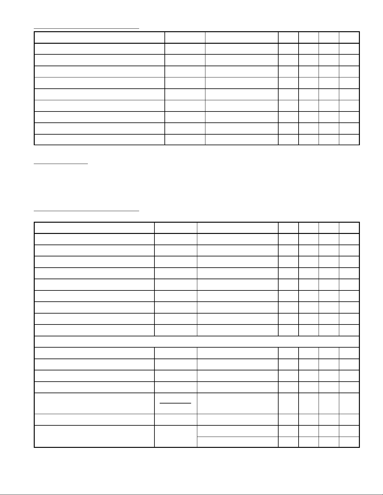
DC Electrical Characteristics: (VCC = 8.5V, TA = +25°C unless otherwise specified)
Parameter Symbol Test Conditions Min Typ Max Unit
Current Consumption (Without LED Driver) I
TOT
Power Dissipation P
Voltages on Pin15 V
Voltages on Pin16, Pin12 V
16–5
DC Current Pin14 –I
DC Current Pin2 –I
Output Current Pin3 –I
Switch “VCO OFF” Voltage (Pin7) V
Current (Pin7) I
D
15–5
, V
14
2
3
7
7
12–5
– 15 – mA
– 125 – mW
– 2.0 – V
– 3.5 – V
195 275 390 µA
195 275 390 µA
– – 20 mA
– 2.2 – V
– – 50 µA
AF Conditions:
Input MUX signal is 1V
= 1kHz; V
P–P
= 32mV (9%), oscillator adjusted t o f
PILOT
= 228kHz at VI = 0V,
OSC
unless otherwise specified. (All figures are measured with a roll–off network of 50kHz (2dB down at
38kHz) at the input.
AC Electrical Characteristics:
Parameter Symbol Test Conditions Min Typ Max Unit
(All parameters are measured in the circuit at nominal supply
voltage(V
= 8.5V) and TA = +25°C)
CC
Gain Input Amplifier A
Input Impedance (External) Z
Maximum Input Voltage V
Gain Output Buffers A
V
I
I
V
– – 20 dB
– 47 – kΩ
– – TBD V
P–P
– 10 – dB
Maximum Output Voltage VO12, 16 THD ≤ 1% – – TBD V
Output Impedance Z
Maximim Load Impedance Z
O
L
Pin12, Pin16 – – 500 Ω
5.0 – – kΩ
Muting Level α muting – 90 – dB
Source Selector α – 90 – dB
Overall Performance
Overall Gain (Mono) V
OUT/VIN
10 11 12 dB
AF Output Voltage (RMS) Mono V12 = V16 1.1 1.25 – V
Total Harmonic Distortion THD V
Output Voltage V
Output Channel Unbalance
12, 16 THD = 1% – – TBD V
OUT
V
12
OUT
V
16
OUT
OUT
= 1.2V
, Note 1 – – 0.5 %
RMS
– 0.2 1.0 dB
Channel Separation α L = 1, R = 0 26 40 – dB
0
Signal–to–Noise Ratio S/N Bandwidth 20Hz to 16kHz – 76 – dB
Bandwidth DINA – 82 – dB
Note 1. Guaranteed for mono, mono +pilot, stereo.
 Loading...