

NTE NTE7048 Datasheet
NTE7048
Integrated Circuit
w
NTSC Decoder
Description:
The NTE7048 is a monolithic integrated decoder for the NTSC color television standard. This device
combines all functions required for the identification and demodulation of NTSC signals ina 20–Lead
DIP type package. Furthermore, it contains a luminance amplifier, an RGB–matrix and amplifier.
These amplifiers supply output signals up to 5V
crete output stages.
Features:
D Automatic Chrominance Leveling (Avoids Saturation at the Chrominance Input)
D Peaking Circuit with DC Control
D Fast RGB Output Blanking
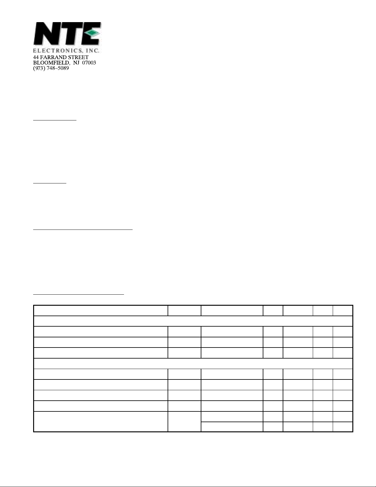
Absolute Maximum Ratings:
Supply Voltage (Pin1), V
Total Power Dissipation, P
Operating Ambient Temperature Range, T
Storage Temperature Range, T
Thermal Resistance, Junction–to–Ambient, R
P
tot
stg
/Fast RGB Blanking
(Picture information) enabling direct drive of dis-
P–P
A
thJA
13.2V. . . . . . . . . . . . . . . . . . . . . . . . . . . . . . . . . . . . . . . . . . . . . . . . . . . . . . . . .
1700mW. . . . . . . . . . . . . . . . . . . . . . . . . . . . . . . . . . . . . . . . . . . . . . . . . . . .
–25° to +65°C. . . . . . . . . . . . . . . . . . . . . . . . . . . . . . . . . . .
–55° to +150°C. . . . . . . . . . . . . . . . . . . . . . . . . . . . . . . . . . . . . . . . . .
50K/W. . . . . . . . . . . . . . . . . . . . . . . . . . . . . . . . . . . .
Electrical Characteristics:
(TA = +25°C, VP = 12V, All voltages referenced to Pin19, unless
otherwise specified)
Parameter Symbol Test Conditions Min Typ Max Unit
Supply (Pin1)
Supply Voltage V
Supply Current I
Total Power Dissipation P
Luminance Amplifier (Pin8)
Input Voltage (Peak–to–Peak Value) V
Input Level before Clipping V
Input Current I
Contrast Control Range – –17 to +3 – dB
Input Current Contrast Control I
P
P
tot
8(P–P)
8
8
6
Note 1 – 450 – mV
V6 < 6V – 0.5 15.0 µA
V6 = 2.5V, Note 2 3 7 – mA
10.8 12.0 13.2 V
– 90 – mA
– 1.08 – W
– – 1.0 V
– 0.15 1.0 µA
Note 1. Signal with negative going sync; amplitude includes sync. pulse amplitude.
Note 2. Peak white limiter active.
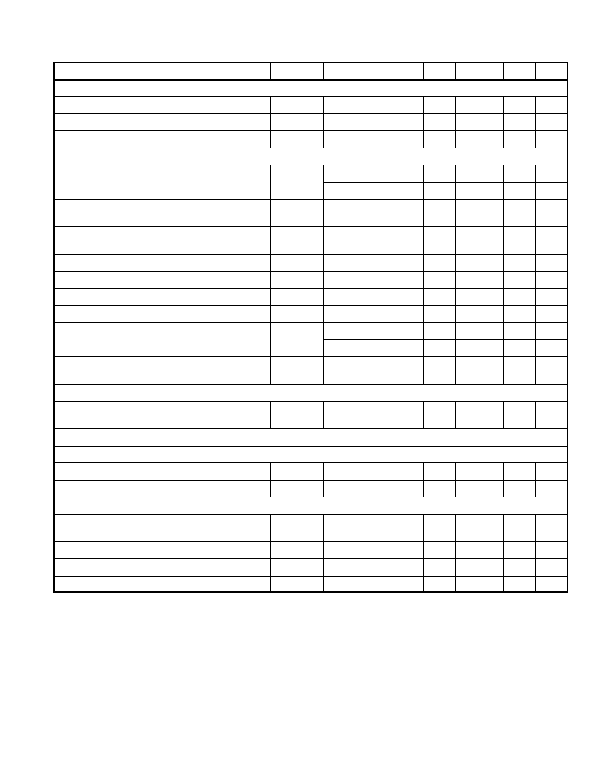
Electrical Characteristics (Cont’d): (TA = +25°C, VP = 12V, All voltages referenced to Pin19, unless
otherwise specified)
Parameter Symbol Test Conditions Min Typ Max Unit
Peaking of Luminance Signal
Input Impedance (Pin15) |Z15| 7 10 13 kΩ
Output Impedance (Pin10) |Z10| 50 75 90 Ω
Luminance Gain Ratio Note 3 – 10 –
Chrominance Amplifier (Pin3)
Input Signal Amplitude (Peak–to–Peak Value) V
3(P–P)
Note 4 – 550 – mV
Note 5 – – 1100 mV
Minimum Burst Signal Amplitude within the ACC
35 – – mV
Control Range (Peak–to–Peak Value)
Change of Red Output Signal over 30dB ACC
∆V
12
– – 2 dB
Control Range
Input Impedance (Pin3) |Z3| 6 9 12 kΩ
Input Capactiance C
3
– 4 6 pF
Saturation Control Range 50 – – dB
Saturation Control Input Current (Pin5) I
5
V5 < 6V – 1 20 µA
Input Impedance (Pin5) |Z5| V5 = 6V to 10V 1.5 2.1 2.7 kΩ
Color Killer Active 1.5 2.1 2.7 kΩ
Tracking Between Luminance and Chrominance
For 10dB of Control – 1 2 dB
Contrast Control
ALC Circuit
Chrominance/Burst Ratio at which ALC
Note 6 – 2.9 –
Commences
Reference Part (Note 7)
Phase–Locked–Loop
Phase–Locked–Loop Catching Range ∆f ±300 ±400 – Hz
Phase Shift for 400Hz Deviation of f
OSC
∆ϕ – – 5 deg
Oscillator (See Note 7)
Oscillator Temperature Coefficient of Oscillator
TC
OSC
– –1.5 –2.5 Hz/K
Frequency
Frequency Deviation ∆f
Input Resistance (Pin18) R
Input Capacitance (Pin18) C
OSC
18
18
∆VP = ±10% – 150 250 Hz
1.0 1.4 1.8 kΩ
– – 10 pF
Note 3. Pin10 AC short–circuit to GND.
Note 4. Ind i c a te d is a s i gnal f or c olor b ar w ith 7 5% s aturation, s o t he c hrominance t o b urst r atio i s 2 .2:1.
Note 5. Before clipping occurs in the input stage.
Note 6. The ALC circuit limits the chromunance amplitude to a particular value as soon as the chro-
minance/burst ratio exceeds 2.9: to 1. The limiting is performed via the ACC function.
Note 7. All frequency variations are referenced to the 3.58MHz carrier frequency.
 Loading...