

NTE NTE7047 Datasheet
NTE7047
Integrated Circuit
TV Color Small Signal Sub System
Features:
D Vision IF Amplifier with Synchronous Demodulator
D Automatic Gain Control (AGC) Detector Suitable for Negative Modulation
D AGC Tuner
D Automatic Frequency Control (AFC) Circuit with Sample–and–Hold
D Video Preamplifier
D Sound IF Amplifier and Demodulator
D DC Volume Control or Separate Supply for Starting the Horizontal Oscillator
D Audio Preamplifier
D Horizontal Synchronization Circuit with Two Control Loops
D Vertical Synchronization (Divider System) and Sawtooth Generation with Automatic Amplitude
Adjustment for 50Hz and 60Hz
D Transmitter Identification (Mute)
D Generation of Sandcastle Pulse
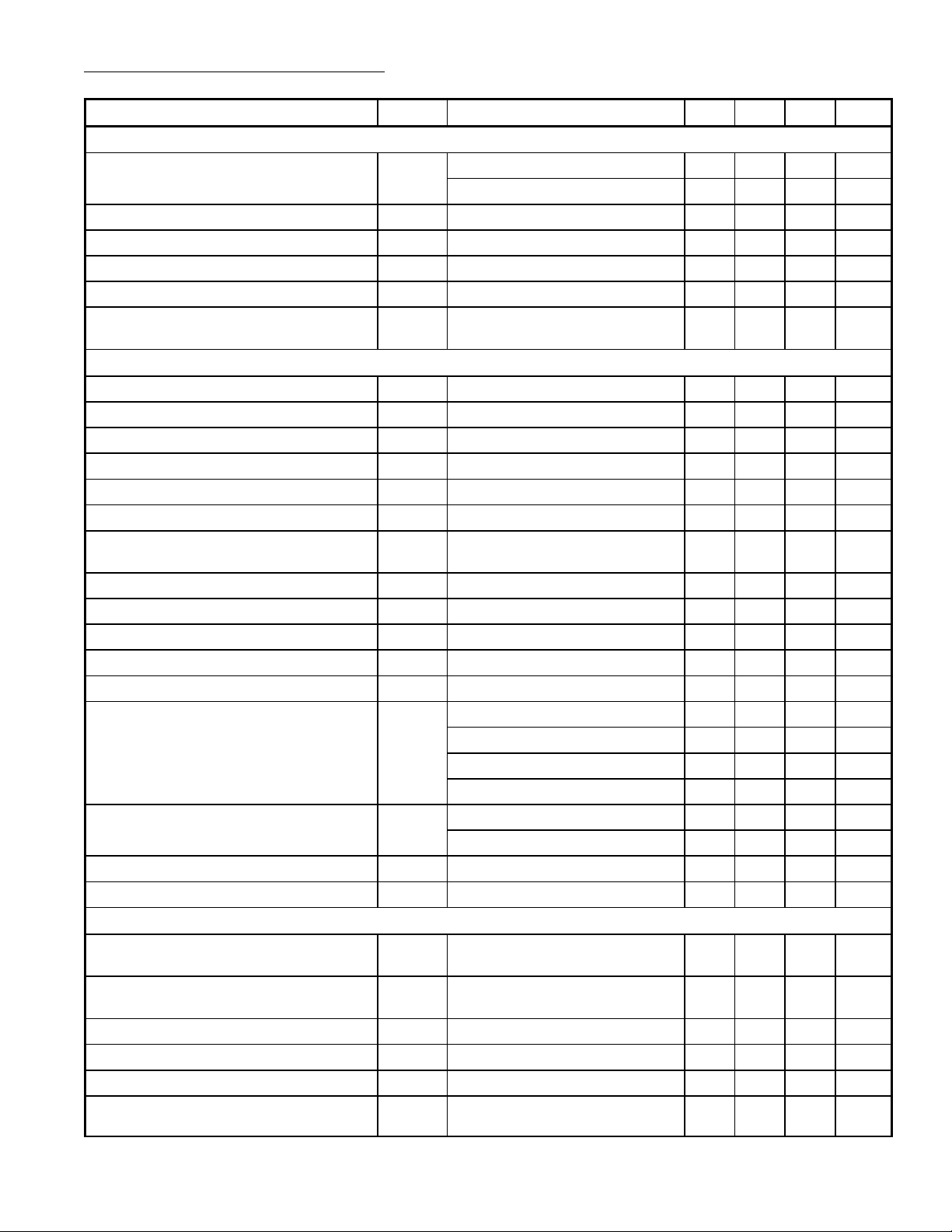
Absolute Maximum Ratings:
Supply Voltage (Pin7), VP = V
Total Power Dissipation, P
7–6
tot
Operating Ambient Temperature Range, T
Storage Temperature Range, T
stg
A
–25° to +65°C. . . . . . . . . . . . . . . . . . . . . . . . . . . . . . . . . . .
–25° to +150°C. . . . . . . . . . . . . . . . . . . . . . . . . . . . . . . . . . . . . . . . . .
13.2V. . . . . . . . . . . . . . . . . . . . . . . . . . . . . . . . . . . . . . . . . . . . . . . . . . .
2.3W. . . . . . . . . . . . . . . . . . . . . . . . . . . . . . . . . . . . . . . . . . . . . . . . . . . . . . . .
Electrical Characteristics: (TA = +25°C, VP = V
= 12V, carrier 38.9MHz, negative modulation
7–6
unless otherwise specified)
Parameter Symbol Test Conditions Min Typ Max Unit
Supplies
Supply Voltage Range (Pin7) V
Supply Current (Pin7) I
Start Current (Pin11) I
Start Voltage Horizontal Oscillator V
Start Protection Level V
7–6
7
11
11
11
At no input 75 125 165 mA
Note 1 – 6.5 9.0 mA
I11 = 12mA – – 16.5 V
9.5 12.0 13.2 V
9.5 – – V
Note 1. Pin11 has a double function. When during switch–on a current of 9mA is supplied to this pin,
it is used to start the horizontal oscillator. The main supply can then be obtained from the
horizontal deflection stage. When no current is supplied to this pin it can be used as a volume
control.
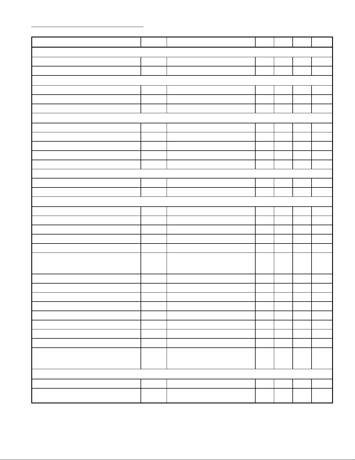
Electrical Characteristics (Cont’d): (TA = +25°C, VP = V
modulation unless otherwise specified)
Parameter Symbol Test Conditions Min Typ Max Unit
Vision IF Amplifier (Pin8 and Pin9)
= 12V, carrier 38.9MHz, negative
7–6
Input Sensitivity (RMS Value) V
At 38.9MHz, Note 2 25 40 60 µV
8–9
At 45.75MHz, Note 2, Note 26 25 40 60 µV
Differential Input Resistance R
Differential Input Capacitance C
Gain Control Range G
Maximum Input Signal V
Output Signal Expansion for 48dB
∆V
Note 3 – 1300 – Ω
8–9
Note 3 – 5 – pF
8–9
8–9
8–9
Note 4 – 1 – dB
17
– 77 – dB
100 170 – mV
Variation of Input Signal
Video Amplifier (Note 5)
Zero Signal Output Level V
Top Sync Level V
Video Output Signal Amplitude V
Note 6 – 50.4 – V
17
17
Note 7 2.3 2.65 3.0 V
17
2.3 2.5 2.7 V
White–Spot Threshold Level – 5.7 – V
White–Spot Insertion Level – 3.8 – V
Video Output Impedance – 25 – Ω
Internal Bias Current of Output Transistor
I
17(int)
1.4 1.8 – mA
(NPN Emitter Follower)
Maximum Source Current I
17
10 – – mA
Bandwidth of Demodulated Output Signal B 5 7 – MHz
Differential Gain G
Note 8 – 4 8 %
17
Differential Phase j Note 8 – 2 5 deg.
Video Non–Linearity NL Note 9 – 2 5 %
Intermodulation f = 1.1MHz (Blue), Note 10 50 60 – dB
f = 1.1MHz (Yellow), Note 10 50 60 – dB
f = 3.3MHz (Blue), Note 10 55 65 – dB
f = 3.3MHz (Yellow), Note 10 55 65 – dB
Signal–to–Noise Ratio S/N Vi = 10mV, Note 11 50 57 – dB
End of gain control range, Note 11 50 62 – dB
Residual Carrier Signal V
Residual 2nd Harmonic of Carrier Signal V
17
17
– 2 10 mV
– 2 10 mV
Tuner AGC
Minimum Starting Point Tuner Take–Over
V
8–9(rms)
(RMS Value)
Maximum Starting Point Tuner Take–Over
V
8–9(rms)
(RMS Value)
Maximum Tuner AGC Output Swing I
5(max)V5
Output Saturation Voltage V
Leakage Current (Pin5) I
Input Signal Variation Complete Tuner
Control
5(sat)I5
L
∆V
i
– – 0.2 mV
100 150 – mV
= 3V 4 – – mA
= 2mA – – 300 mV
– – 1 µA
0.5 2.0 4.0 dB
Electrical Characteristics (Cont’d): (TA = +25°C, VP = V
= 12V, carrier 38.9MHz, negative
7–6
modulation unless otherwise specified)
Parameter Symbol Test Conditions Min Typ Max Unit
Tuner AGC (Cont’d)
Minimum Voltage Tuner Take–Over V
Voltage to Switch on the X–Ray Protection V
1
Horizontal output high resistance – – 0.8 V
1
AFC Circuit (AFC Sample–and–Hold/Switch)
AFC Switch–Off Current I
Output Current I
Leakage Current at Pin19 I
19
19
LO
V19 = 0V – 0.1 0.3 mA
AFC Circuit (AFC Output)
AFC Output Voltage Swing V
Available Output Current I
Note 12, Note 13 10.5 – 11.5 V
18
18
Control Steepness – 100 – mV/kHz
AFC Output Voltage with AFC Off V
AFC Output Resistance R
18
18
Measured With an Input Signal Amplitude = 150µV (RMS value)
Output Voltage Swing V
Note 26 – 11 – V
18
Control Steepness Note 26 – 80 – mV/kHz
Sound Circuit (Note 14)
Input Limiting Voltage V
Input Resistance R
Input Capacitance C
15
15
15
V
o(max)
= –3dB – 400 800 µV
AM Suppression AMS 53 58 – dB
AF Output Signal (RMS Value) V
AF Output Signal when Pin11 is used as
12(rms)
V
12(rms)
Note 15 400 600 800 mV
∆f = 50kHz 500 900 1500 mV
a Starting Pin or Connected to
VP (RMS Value)
AF Output Impedance Z
12
Total Harmonic Distortion THD Note 16 – 0.5 2.0 %
Ripple Rejection RR Volume control 20dB; fk = 100Hz – 35 – dB
Output Voltage When Muted V
Output Level Shift due to Muting V
12
Volume control –20dB – – 0.5 V
12
Signal–to–Noise Ratio S/N Note 17 – 47 – dB
Voltage with Pin11 Disconnected V
Current with Pin11 Short Circuited to GND I
Temperature Dependence of the Output
Signal Amplitude
11
11
V
TA = +20° to +65°C,
12
–30dB volume control and
voltage of Pin11 fixed, Note 26
Volume Control (Note 18)
External Control Resistor R
Suppression Output Signal during
OSS 60 66 – dB
Note 18 – 4.7 – kΩ
11
Mute Condition
– – 1 V
0.1 – – mA
– – 2 µA
0.2 – – mA
5.5 6.0 6.5 V
– 40 – kΩ
– 2.6 – kΩ
– 6 – pF
– 25 100 Ω
– 2.5 – V
– 6.0 – V
– 1 – mA
– 2.5 – dB
 Loading...