

NTE NTE7040 Datasheet

NTE7040
Integrated Circuit
Audio Power Amplifier, 20W
Features:
D High Output Power:
20W Typ (±B1 = ±22V, RL = 8Ω, f = 20Hz to 20kHz, THD = 1%)
18W Typ (±B1 = ±22V, RL = 8Ω, f = 20Hz to 20kHz, THD = 0.5%)
where: ±B1: Supply Voltage, RL: Load Frequency, f: Frequency,
THD: Total Harmonic Distortion, ±B2 = 25V constant
D Very Low Harmonic and Crossover Distortion:
0.02% Typ (±B1 = ±22V, RL = 8Ω, f = 1kHz, P
0.04% Typ (±B1 = ±22V, RL = 8Ω, f = 20Hz to 20kHz, P
D Wide Frequency Range: From 5Hz to 120kHz (at –1dB frequency response)
D Thermal Shut–down Circuit Included
D Muting Circuit Included
Absolute Maximum Ratings: (TA = +25°C unless otherwise specified)
Positive Supply Voltage (Note 1), +B1, +B
Negative Supply Voltage (Note 1), –B
Output Current, I
Input Voltage, V
Power Dissipation (TC = +60°C), P
Junction Temperature, T
Operating Temperature Range, T
Storage Temperature Range, T
O(peak)
i(peak)
T
J
opr
stg
Thermal Resistance, Junction–to–Case, R
2
1
thJC
= 2W)
out
= 2W)
out
30V. . . . . . . . . . . . . . . . . . . . . . . . . . . . . . . . . . . . . . . . . . . .
–30V. . . . . . . . . . . . . . . . . . . . . . . . . . . . . . . . . . . . . . . . . . . . . . .
7.5A. . . . . . . . . . . . . . . . . . . . . . . . . . . . . . . . . . . . . . . . . . . . . . . . . . . . . . . . . . . .
±10V. . . . . . . . . . . . . . . . . . . . . . . . . . . . . . . . . . . . . . . . . . . . . . . . . . . . . . . . . . . . . .
30W. . . . . . . . . . . . . . . . . . . . . . . . . . . . . . . . . . . . . . . . . . . . . . . . .
+150°C. . . . . . . . . . . . . . . . . . . . . . . . . . . . . . . . . . . . . . . . . . . . . . . . . . . . . . . .
–20° to +70°C. . . . . . . . . . . . . . . . . . . . . . . . . . . . . . . . . . . . . . . . .
–55° to +125°C. . . . . . . . . . . . . . . . . . . . . . . . . . . . . . . . . . . . . . . . . .
2.5°C/W. . . . . . . . . . . . . . . . . . . . . . . . . . . . . . . . . . . . .
Note 1. Standard operating voltages are as follows: +B2 = +25V, ±B1 = ±22V, ±19V
Electrical Characteristics: (TA = +25°C, ±B1 = ±25V, +B2 = 25V, RL = 8Ω, Rg = 600Ω unless
otherwise specified)
Parameter Symbol Test Conditions Min Typ Max Unit
Quiescent Current +I
+I
–I
Output Offset Voltage ∆V
Input Resistance R
Voltage Gain (Closed Loop) G
Voltage Gain (Open Loop) G
Output Power P
V(OL)
O1
P
O2
Total Harmonic Distortion THD f = 20kHz, P
Output Noise Voltage V
Supply Voltage Rejection Ratio SVR Rg = 5.1kΩ, f
Vin = 0 between +B1 and Pin5 20 60 120 mA
Q1
Q2
Q1
Vin = 0, between Pin3 and GND – 0 ±0.1 V
O
f = 1kHz, R
in
f = 1kHz, R
V
f = 1kHz, R
f = 20kHz,
Note 2
Rg = 5.1kΩ, BW = 20Hz to 20kHz – 0.35 0.50 mV
n
between +B2 and Pin6 – – 22 mA
between –B1 and Pin1 2 – – 152 mA
= 56kΩ – 55 – kΩ
102
= 680Ω, R
103
= 0 – 88 – dB
103
= 56kΩ – 38 – dB
104
THD = 0.5%, RL = 8Ω 15 18 – W
THD = 0.7%, RL = 4Ω 15 18 – W
= 2W – 0.04 0.20 %
out
= 100Hz (at Pin12) 52 60 – dB
ripple
Note 2. Standard test conditions are as follows: PO1: ±B1 = ±22V, PO2: ±B1 = ±19V
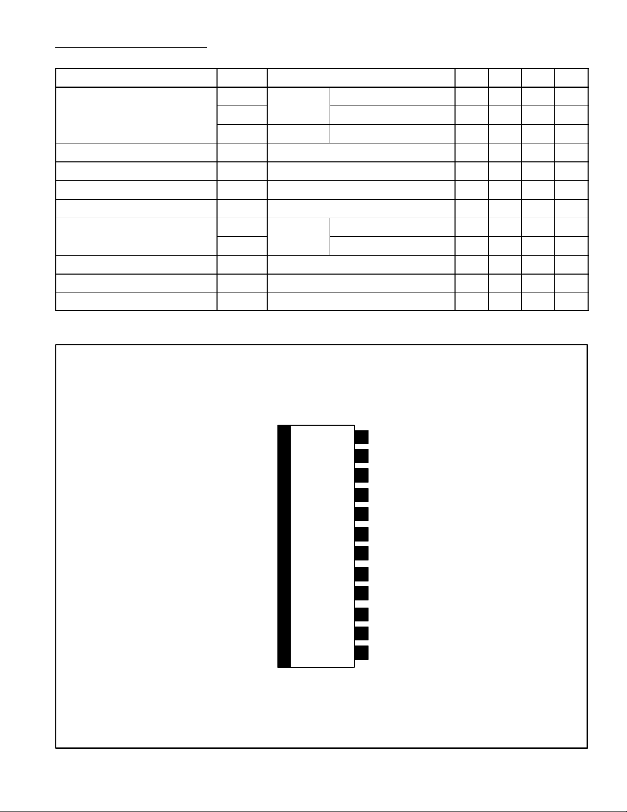
Pin Connection Diagram
(Front View)
12
GND
11
Ripple Rejection
10
Input
Input
9
Compensation
8
7
G
N
D
Compensation
6
Muting Input
5
V
CC
4
N.C.
3
Output
2
N.C.
N.C.1
 Loading...