

NTE NTE704 Datasheet
NTE704
Integrated Circuit
TV Sound, IF Amp
Features & Applications:
D Exceptionally High Gain: Power Gain at 4.5Hz – 75dB typ.
D Excellent Limiting Characteristics: Input Limiting Voltage (Knee) = 300µV at 4.5MHz
D Excellent AM Rejection: > 50dB at 4.5MHz
D High Audio–Voltage Recovery: 20mV Typ at 4.5MHz, 25kHz Deviation
D Wide Frequency Capability: 100kHz to > 20MHz
D Comprehensive Circuit Functions:
IF Amplifier
AM and Noise Limiter
FM Detector
Audio PreAmplifier
Absolute Maximum Ratings
: (TA = +25°C unless otherwise specified)
Maximum Input–Signal Voltage (Between Pin1 and Pin2) ±3V. . . . . . . . . . . . . . . . . . . . . . . . . . . . . . . .
Maximum Device Dissipation 300mW. . . . . . . . . . . . . . . . . . . . . . . . . . . . . . . . . . . . . . . . . . . . . . . . . . . .
Recommended Minimum DC Supply Voltage (V
CC
) 5.5V. . . . . . . . . . . . . . . . . . . . . . . . . . . . . . . . . . . .
Operating Temperature Range, T
opr
–55° to +125°C. . . . . . . . . . . . . . . . . . . . . . . . . . . . . . . . . . . . . . . .
Storage Temperature Range, T
stg
–65° to +150°C. . . . . . . . . . . . . . . . . . . . . . . . . . . . . . . . . . . . . . . . . .
Electrical Characteristics
: (TA = +25°C unless otherwise specifid)
Parameter Symbol Test Conditions Min Typ Max Unit
Total Device Dissipation P
T
Note 1 VCC = 6V 73 90 110 mW
VCC = 7.5V 106 120 150 mW
VCC = 10V 165 190 230 mW
Voltage Gain A
f = 1Mc/s,
VCC = 6V 60 66 – dB
Note 2
VCC = 7.5V 65 70 – dB
VCC = 10V 65 71 – dB
VCC = 7.5V,
f = 4.5Mc/s 60 67 – dB
Note 2
f = 10.7Mc/s 55 60 – dB
Note 1. Total current drain may be determined by dividing PT by VCC.
Note 2. Recommended minimum DC supply voltage (V
CC
) is 5.5V. Nominal load current flowing into
Pin5 is 1.5mA at 7.5V.
Electrical Characteristics (Cont’d): (TA = +25°C unless otherwise specifid)
Parameter Symbol Test Conditions Min Typ Max Unit
Parallel Input Resistance R
IN
f = 4.5Mc/s, VCC = 7.5V – 3 – kΩ
Parallel Input Capacitance C
IN
– 7 – pF
Parallel Output Resistance R
OUT
f = 4.5Mc/s, VCC = 7.5V – 31.5 – kΩ
Parallel Output Capacitance C
OUT
– 4.2 – pF
Noise Figure NF f = 4.5Mc/s, VCC = 7.5V – 8.7 – dB
Input Limiting Voltage (Knee) V
i(lim)
f = 4.5Mc/s, VCC = 7.5V – 300 400 µV
Recovered AF V
o(af)
f = 4.5Mc/s VCC = 6V – 155 – mV
VCC = 7.5V 135 188 – mV
VCC = 10V – 220 – mV
Amplitude Modulation Rejection AMR f = 4.5Mc/s, VCC = 7.5V – 50 – dB
Discriminator Output Resistance RO(dics) f = 4.5Mc/s, VCC = 7.5V – 60 – Ω
Total Harmonic Distortion THD f = 4.5Mc/s, VCC = 7.5V – 1.8 – %
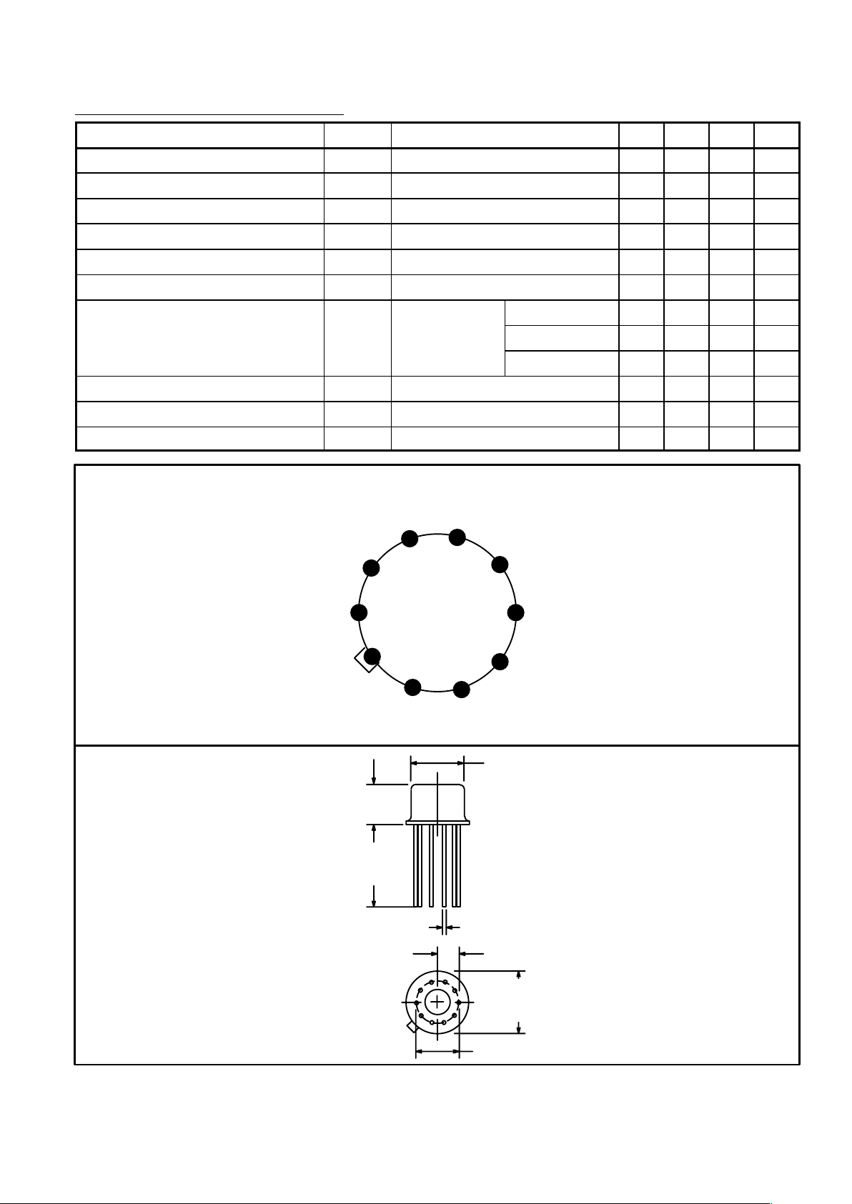
Pin Connection Diagram
(Top View)
10
9
8
5
4
3
2
7
6
1
Bypass
Input 4.5MH
Z
Primary Discrimin
Transformer/V
CC
(+)
Secondary Discrim
Transformer
Secondary Discrimin
Transformer
Primary Discrimin
Transformer
Tertiary Winding
GND
Input 4.5MH
Z
Output
4
.018 (0.45) Dia Typ
.335 (8.52) Dia Max
.115 (2.92)
.230 (5.84) Dia
.260
(6.6)
Max
.500
(12.7)
Min
.370
(9.4)
Max
1
2
3
4
5
6
7
8
9
10
 Loading...