

NTE NTE7030 Datasheet
NTE7030
Integrated Circuit
Module, AF PO, 50W,
Dual Power Supply
Features:
D Small–Sized Package Allows Audio Sets to be made Slimmer
D Facilitates Thermal Design of Slim Stereo Sets
D Constant–Current Circuit Minimizes Pop Noise During Power ON/OFF
D Possible to Design Electronic Supplementary Circuits:
Pop Noise Muting During Power ON/OFF
Load Short–Circuit Protector
Thermal Shutdown
Absolute Maximum Ratings:
Maximum Supply Voltage, V
Junction Temperature, T
J
Operating Case Temperature, T
Storage Temperature Range, T
Thermal Resistance, Junction–to–Case, R
Available Time for Load Shorted (V
Recommended Operating Conditions:
Recommended Supply Voltage, V
Load Resistance, R
L
Electrical Characteristics:
Parameter Symbol Test Conditions Min Typ Max Unit
Quiescent Current I
Output Power P
Total Harmonic Distortion THD PO = 1W, f = 1kHz – – 0.3 %
Frequency Response fL, f
Input Resistance r
Output Noise Voltage V
Middle–Point Voltage V
(TA = +25°C unless otherwise specified)
max ±52V. . . . . . . . . . . . . . . . . . . . . . . . . . . . . . . . . . . . . . . . . . . . . . . . . .
CC
+150°C. . . . . . . . . . . . . . . . . . . . . . . . . . . . . . . . . . . . . . . . . . . . . . . . . . . . . . . . .
C
stg
thJC
= ±35V, RL = 8Ω, f = 50Hz, PO = 50W), t
CC
–30° to +125°C. . . . . . . . . . . . . . . . . . . . . . . . . . . . . . . . . . . . . . . . . .
s
+125°C. . . . . . . . . . . . . . . . . . . . . . . . . . . . . . . . . . . . . . . . . . . . . . . . . .
1.8°C/W. . . . . . . . . . . . . . . . . . . . . . . . . . . . . . . . . . . . .
(TA = +25°C unless otherwise specified)
CC
(TA = +25°C, VCC = ±35V, RL = 8Ω (Non–Inductive Load), Rg = 600Ω,
= 40dB unless otherwise specified)
V
G
CCO
O
i
NO
N
VCC = ±42V
THD = 0.4%, f = 20Hz to 20kHz 50 – – W
VCC = ±31V, THD = 1%, R
PO = 1W +0dB, –3dB 20 to 50k Hz
H
PO = 1W, f = 1kHz – 55 – kΩ
VCC = ±42V, R
VCC = ±42V
= 10kΩ, Note 2
g
= 4Ω, f = 1kHz
L
10 20 50 mA
55 – – W
– – 1.2 mV
–70 0 +70 mV
2sec. . . . . . . . . . .
±35V. . . . . . . . . . . . . . . . . . . . . . . . . . . . . . . . . . . . . . . . . . . . . . . . .
8Ω. . . . . . . . . . . . . . . . . . . . . . . . . . . . . . . . . . . . . . . . . . . . . . . . . . . . . . . . . . . . . . . . .
rms
Note 1. For power supply at the time of test, use a onstant–voltage power supply unless otherwise
specified.
Note 2. The output noise voltage represents the peak value on the RMS scale (V
) of average
TMV
value indicating type. The noise voltage waveform includes no flicker noise.
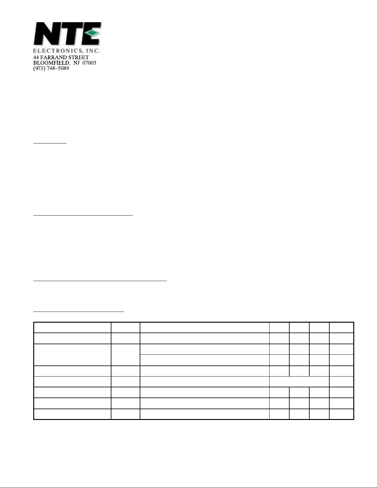
Pin Connection Diagram
(Front View)
Bootstrap
15
14
(+) V
13
Output
(–) V
12
11 Compensation
10
I Adjust
9
Emitter Bypass
8
Compensation
7
I Adjust
Test Point
6
5
Bypass
4
Bias
Substrate
3
NFB
2
Input
1
CC
CC
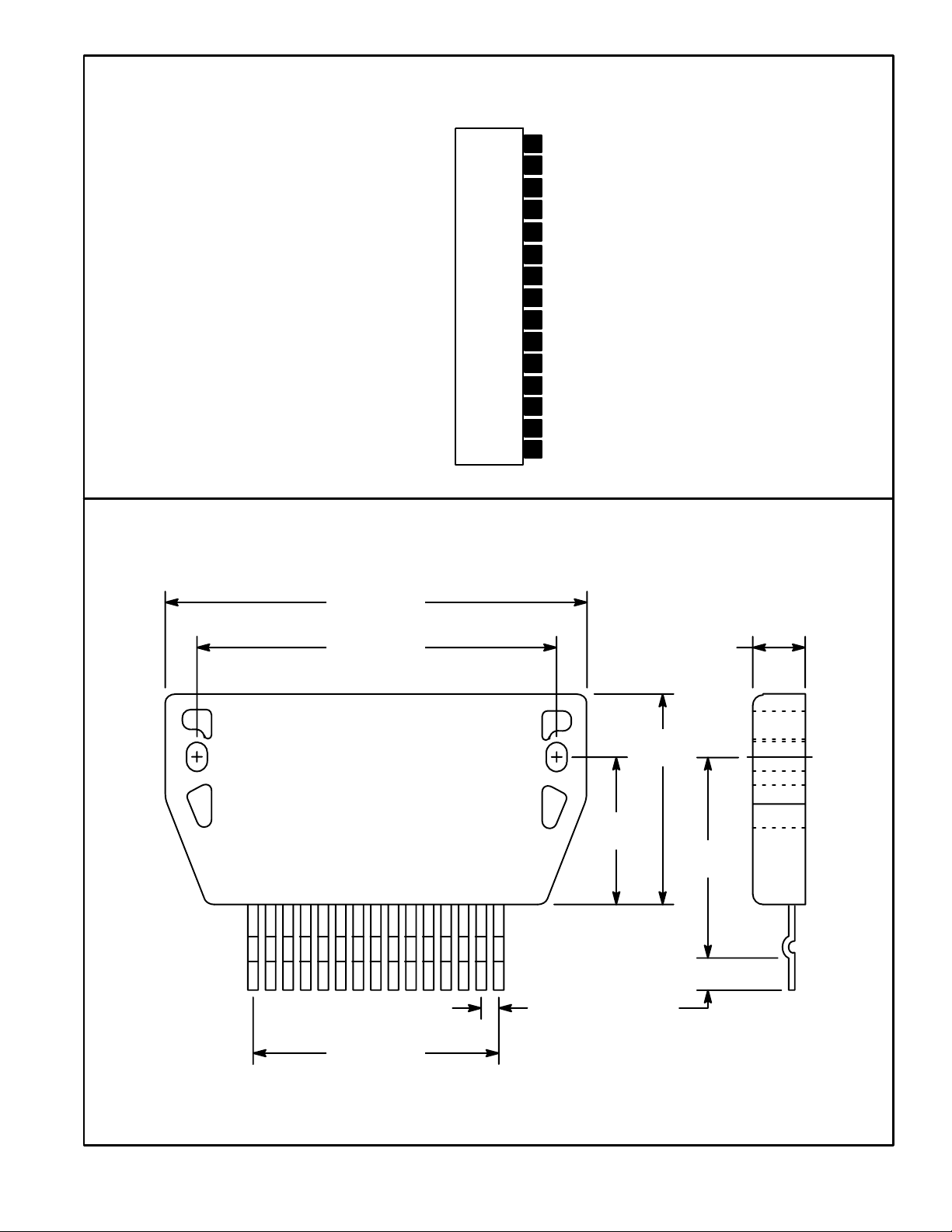
2.330 (59.2)
2.050 (52.0)
.335 (8.5)
1.230
(31.2)
.827
(21.0)
1.110
(28.0)
115
.100 (2.54)
.158 (4.0)
1.400 (35.6)
 Loading...