

NTE NTE7016 Datasheet

NTE7016
Integrated Circuit
FM IF System
Description:
The NTE7016 is a monolithic integrated circuit that provides all the functions of a comprehensive FM–
IF system. This device includes a three–stage FM–IF amplifier/limiter configuration with level detectors for each stage, a doubly–balanced quadrature FM detector, and an audio amplifier that features
the optional use of a muting (squelch) circuit.
The advanced circuit design of the IF system includes desirable deluxe features such as programmable delayed AGC for the RF tuner , an AFC drive circuit, and an output signal to drive a tuning meter
and/or provide stereo switching logic. In addition, internal power supply regulators maintain a nearly
constant current drain over the voltage supply range of +8.5 to +16 volts.
The NTE7016 is ideal for high fidelity operation. Distortion in an NTE7016 FM–IF System is primarily
a function of the phase linearity characteristic of the outboard detector coil.
The NTE7016 is available in a 16–Lead DIP type plastic package and can operate over the ambient
temperature range of –40°C to +85°C.
Features:
D Exceptional Limiting Sensitivity: 12µV typ. at –3db Point
D Low Distortion: 0.1% typ. (With Double–Tuned Coil)
D Single–Coil Tuning Capability
D Improved S + N/N Ratio
D Externally Programmable Recovered Audio Level
D Provides Specific Signal for Control of Interchannel Muting (Squelch)
D Provides Specific Signal for Direct Drive of a Tuning Meter
D On Channel Step for Search Control
D Provides Programmable AGC Voltage for RF Amplifier
D Provides a Specific Circuit for Flexible Audio Output
D Internal Supply Voltage Regulators
D Externally Programmable “ON” Channel Step Width, and Deviation at Which Muting Occurs
Absolute Maximum Ratings: (TA = +25°C unless otherwise specified)
DC Supply Voltage (Between Pin11 and Pin4) 16V. . . . . . . . . . . . . . . . . . . . . . . . . . . . . . . . . . . . . . . .
(Between Pin11 and Pin14) 16V. . . . . . . . . . . . . . . . . . . . . . . . . . . . . . . . . . . . . . .
DC Current (Out of Pin15) 2mA. . . . . . . . . . . . . . . . . . . . . . . . . . . . . . . . . . . . . . . . . . . . . . . . . . . . . . . . . .
Device Dissipation, P
D
Up to TA = +85°C 640mW. . . . . . . . . . . . . . . . . . . . . . . . . . . . . . . . . . . . . . . . . . . . . . . . . . . . . . . . .
Derate linearly above TA = +85°C 9.9mW/°C. . . . . . . . . . . . . . . . . . . . . . . . . . . . . . . . . . . . . . . .
Operating Ambient Temperature Range, T
Storage Temperature Range, T
Lead Temperature (During Soldering), T
stg
L
opr
–40° to +85°C. . . . . . . . . . . . . . . . . . . . . . . . . . . . . . . . . .
–65° to +150°C. . . . . . . . . . . . . . . . . . . . . . . . . . . . . . . . . . . . . . . . . .
(At a distance not less than 1/32” (0.79mm) from case for 10sec max) +265°C. . . . . . . . . . .
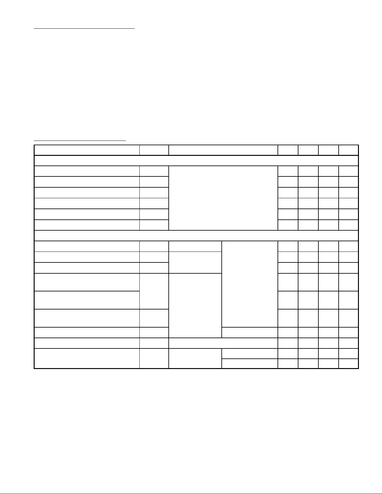
Electrical Characteristics:
(TA = +25°C, V+ = 12V unless otherwise specified)
Parameter Symbol Test Conditions Min Typ Max Unit
Static (DC) Characteristics
Quiescent Circuit Current I
IF Input (Pin1) V
AC Return to Input (Pin2) V
DC Bias to Input (Pin3) V
RF AGC (Pin15) V
DC Reference (Pin10) V
11
1
2
No Signal Input, Non Muted
3
15
10
20 31 40 mA
1.2 1.9 2.4 V
1.2 1.9 2.4 V
1.2 1.9 2.4 V
7.5 9.5 11.0 V
5.0 5.6 6.0 V
Dynamic Characteristics
Input Limiting Voltage (–3dB Point) VI(lim) – 12 25 µV
AM Rejection (Pin6) AMR
Recovered AF Voltage (Pin6) VO(AF)
Total Harmonic Distortion:
Single Tuned (Pin6) Note 1
Total Harmonic Distortion:
THD
Double Tuned (Pin6) Note 1
Signal Plus Noise to Noise Ratio
S + N/N
VIN = 0.1V,
VIN = 0.1V,
AM Mod. = 30%
VIN = 0.1V
VIN = 0.1V
fO = 10.7MHz,
= 400Hz,
f
mod
Deviation ±75kHz
45 55 – dB
325 500 650 mV
– 0.5 1.0 %
– 0.1 – %
65 72 – dB
(Pin6)
Deviation Mute Frequency f
RF AGC Threshold V
ON Channel Step V
DEV
16
12
VIN = 0.1V f
f
= 0 – ±40 – kHz
mod
– 1.25 – V
< ±40kHz – 0 – V
DEV
f
> ±40kHz – 5.6 – V
DEV
Note 1. THD characteristics are essentially a function of the phase characteristics of the network
connected between Pin8, Pin9, and Pin10.
 Loading...