

NTE NTE7013 Datasheet

NTE7013
Integrated Circuit
Remote Control Preamp with Active “Low”
Description:
The NTE7013 is a bipolar integrated circuit in an 8–Lead DIP type package intended for infrared remote control applications. This device has an active “Low” output polarity and contains a high–gain
amplifier, a limiter amplifier, a band–pass filter, a detector, and a pulse shaper.
Features:
D On–Chip Band–Pass Filter: Frequenct Range 30 to 60kHz
D High Gain Pre–Amplifier: 86dB Typ
D Detector for PCM Demodulation
D Low Current Consumption
D Minimum External Components
Absloute Maximum Ratings:
Supply Voltage (R
Output Voltage, V
Input Voltage, V
Supply Current, I
Power Dissipation, P
= 0Ω), V
g
OUT
. . . . . . . . . . . . . . . . . . . . . . . . . . . . . . . . . . . . . . . . . . . . . . . . . . . . . . . . . . . . . . . .
IN
CC
D
Operating Temperature Range, T
Storage Temperature Range, T
(TA = +25°C unless otherwise specified)
CC
opr
stg
Recommended Operating Conditions:
Parameter Symbol Test Conditions Min Typ Max Unit
Power Supply Voltage V
Power Supply Voltage V
Operating Frequency f
CC
CC’
O
Rg = 0Ω 4.5 5.0 5.5 V
Rg = 1.5kΩ 11 12 13 V
5.6V. . . . . . . . . . . . . . . . . . . . . . . . . . . . . . . . . . . . . . . . . . . . . . . . . . . . . .
15V. . . . . . . . . . . . . . . . . . . . . . . . . . . . . . . . . . . . . . . . . . . . . . . . . . . . . . . . . . . . . . .
5V
P–P
6mA. . . . . . . . . . . . . . . . . . . . . . . . . . . . . . . . . . . . . . . . . . . . . . . . . . . . . . . . . . . . . . . .
270mW. . . . . . . . . . . . . . . . . . . . . . . . . . . . . . . . . . . . . . . . . . . . . . . . . . . . . . . . . .
–20° to +75°C. . . . . . . . . . . . . . . . . . . . . . . . . . . . . . . . . . . . . . . . .
–40° to +125°C. . . . . . . . . . . . . . . . . . . . . . . . . . . . . . . . . . . . . . . . . .
30 – 60 kHz
Electrical Characteristics: (TA = +25°C, VCC = 5V unless otherwise specified)
Parameter Symbol Test Conditions Min Typ Max Unit
Power Supply Current I
Input Pin Voltage 1 V
Input Pin Voltage 2 V
Voltage Gain A
Frequency Response A
Input Impedance r
Output Pulse Width 1 t
Output Pulse Width 2 t
Output Voltage V
Output Leak Current I
CC
IN1
IN2
ν
ν
Q
in
PW1
PW2
OL
OH
I1 = –100µA 0.5 0.9 1.7 V
38kHz CW, νi = 30µV
28, 35, 41, 48kHz CW, νi = 30µV
38kHz CW, νi = 0.2V
38kHz Burst, νi = 60µV
VCC = 4V, 38kHz Burst, νi = 50µV
E1 = 1.0V – 0.2 0.4 V
E1 = 2.5V, E2 = 15V – – 2.0 µA
Note 1. Voltage gain difference A
A
47
Note 2. r
=
in
v
i/vx
(kΩ), vx: Input voltage, vi: SG output voltage
–1
P–P
, Note 2 27 40 55 kΩ
P–P
P–P
= Aν (35kHz) – Aν (28kHz)
ν
Q
= Aν (41kHz) – Aν (48kHz)
ν
Q
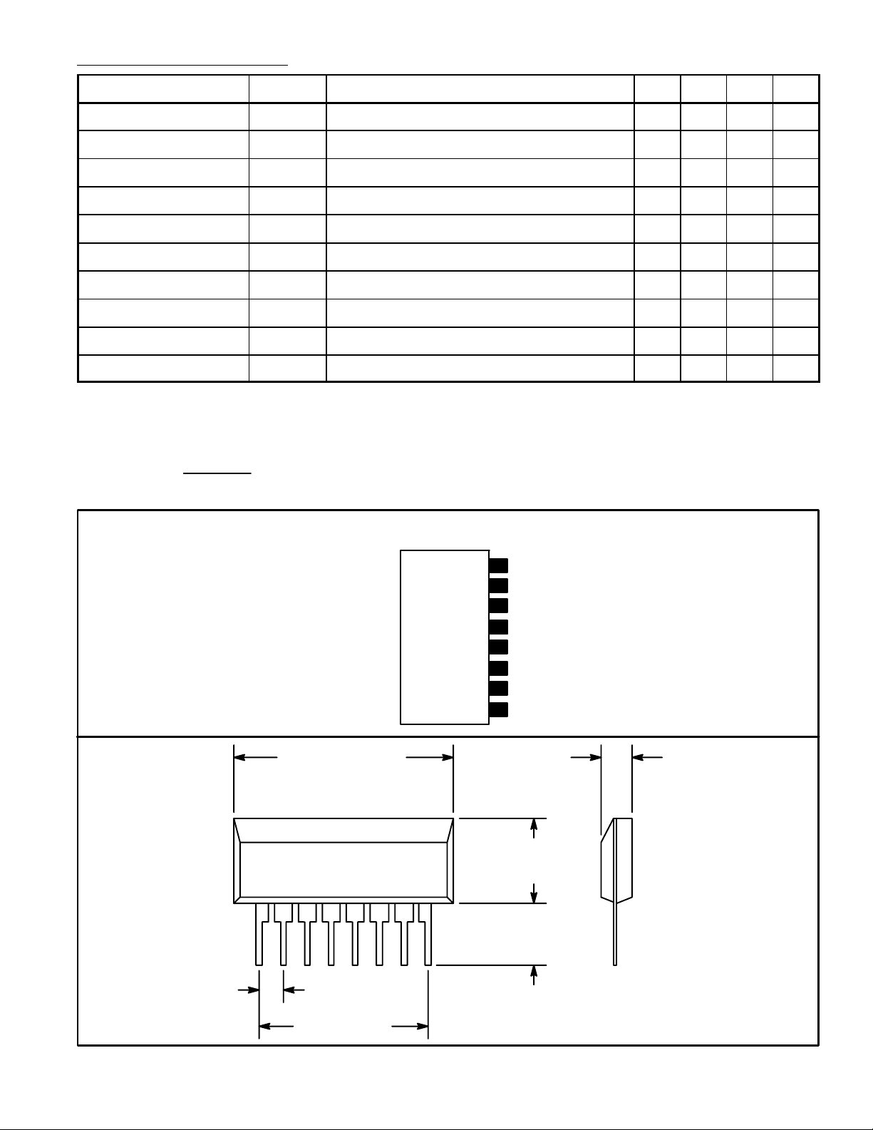
Pin Connection Diagram
(Front View)
– 1.6 2.5 mA
2.0 2.5 3.1 V
74 86 89 dB
, Note 1 4 10 – dB
P–P
440 – 770 µs
P–P
440 – 770 µs
Input (+)
8
7
Input (–)
6
CD
5
GND
4
FO
C1/Filter
3
2
Output
V
1
CC
.768 (19.52) Max .118 (3.0) Max
.264 (6.72)
Max
18
.165 (4.2)
Min
.100 (2.54) Typ
.700 (17.78)
 Loading...