

NTE7005
Integrated Circuit
2–Phase Stepping Motor Driver
Description:
The NTE7005 monolithic power IC is a dual bridge driver in a 16–Lead DIP type package. The maximum driving current and voltage is 330mA x 12V per bridge. Therefore, the best use for this part is
in a two–phase bipolar stepping motor driving the head actuator of a 3, to 5.25–inch Floppy Disk Drive.
Features:
D 330mA Output Current Capability
D Dual Bridge Included
D Power Save
D Single Input Direction Control
D Low Output Saturation Voltage
D Low Supply Current
D Low Input Current
D Compatible with TTL, LSTTL, and 5V CMOS
D Thermal Shutdown
Absolute Maximum Ratings
Logic Stage Supply Voltage, V
Seeking Supply Voltage, V
Holding Supply Voltage, V
Input Voltage, V
. . . . . . . . . . . . . . . . . . . . . . . . . . . . . . . . . . . . . . . . . . . . . . . . . . . . . . . . . . . . . . . .
i
Peak Seeking Current (t ≤ 5ms), I
DC Seeking Current, I
DC Holding current, I
os
OH
Power Dissipation (Note 2), P
Junction Temperature, T
Operating Junction Temperature Range, T
Storage Temperature Range, T
: (TA = +25°C, Note 1 unless otherwise specified)
CC
s1
s2
(peak) 500mA. . . . . . . . . . . . . . . . . . . . . . . . . . . . . . . . . . . . . . . . . . .
o
T
J
opr
stg
7V. . . . . . . . . . . . . . . . . . . . . . . . . . . . . . . . . . . . . . . . . . . . . . . . . . . . . .
15V. . . . . . . . . . . . . . . . . . . . . . . . . . . . . . . . . . . . . . . . . . . . . . . . . . . . . . . . .
7V. . . . . . . . . . . . . . . . . . . . . . . . . . . . . . . . . . . . . . . . . . . . . . . . . . . . . . . . . .
0 to V
CC
330mA. . . . . . . . . . . . . . . . . . . . . . . . . . . . . . . . . . . . . . . . . . . . . . . . . . . . . . . . . .
200mA. . . . . . . . . . . . . . . . . . . . . . . . . . . . . . . . . . . . . . . . . . . . . . . . . . . . . . . . . .
2W. . . . . . . . . . . . . . . . . . . . . . . . . . . . . . . . . . . . . . . . . . . . . . . . . . . . . . .
+150°C. . . . . . . . . . . . . . . . . . . . . . . . . . . . . . . . . . . . . . . . . . . . . . . . . . . . . . . . .
–20° to +125°C. . . . . . . . . . . . . . . . . . . . . . . . . . . . . . . .
–55° to +125°C. . . . . . . . . . . . . . . . . . . . . . . . . . . . . . . . . . . . . . . . . .
Note 1. The absolute maximum ratings are limiting values, to be applied individually, beyond which
the device may be permanently damaged. Functional operation under any of these conditions is not guaranteed. Exposing a circuit to its absolute maximum rating for extended periods of time may affect the device’s reliability.
Note 2. Thermal resistance is as follows:
R
1 ≤ +60°C/W (Soldered on a print circuit board)
thJA
2 ≤ +35°C/W (Soldered on a print circuit covered with copper sufficiently)
R
thJA
R
3 ≤ +15°C/W (Soldered on Pin4, Pin5, Pin12, and Pin13 with an infinite heat sink)
thJA
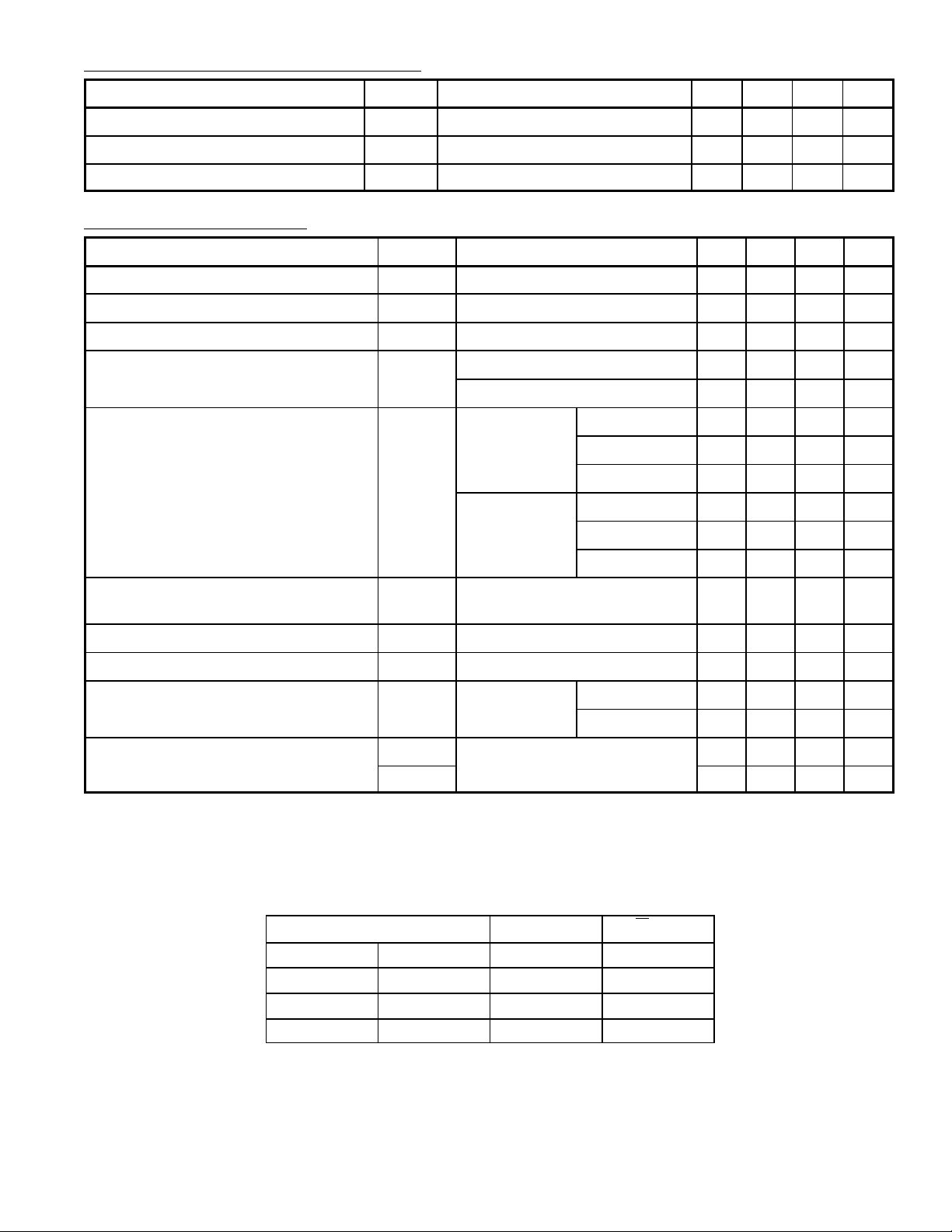
Recommended Operating Conditions:
Parameter Symbol Test Conditions Min Typ Max Unit
Logic Stage Supply Voltage V
Seeking Supply Voltage V
Holding Supply Voltage V
CC
s1
s2
4.5 5.0 5.5 V
10.2 12.0 13.8 V
4.5 5.0 5.5 V
Electrical Characteristics: (TA = +25°C, VCC = 5V, Vs2 = 5V, Vs1 = 12V unless otherwise specified)
Parameter Symbol Test Conditions Min Typ Max Unit
Input Low Voltage V
Input High Voltage V
Input Low Current I
Input High Current I
Supply Current I
IH
IL
IH
CC
IL
VI = 0.8V – – ±10 µA
VI = 2V – 1.0 ±10 µA
VI = 5.5V – 0.5 1.0 mA
PS = 0.8V,
Io = 0
V
CC
Vs1, Note 3 – 10 20 mA
Vs2, Note 4 – – 1.0 mA
PS = 2V,
Io = 0
V
CC
Vs1, Note 3 – 3 5 mA
Vs2, Note 4 – 5 10 mA
– – 0.8 V
2.0 – – V
– 25 33 mA
– 25 33 mA
Output Transistor Breakdown Voltage V
Vs1 Saturation Voltage V
Vs2 Saturation Voltage V
(BR)CE
CE(sat)
CE(sat)
Clamp Diode Forward Voltage V
Delay Time t
t
R
PLH
PHL
IC = 10mA 18 – – V
1 PS = 0.8V, Io = 330mA, Note 5 – 1.5 2.0 V
2 PS = 2V, Io = 130mA, Note 5 – 1.5 2.0 V
IF = 330mA Upper – 5 – V
F
Io = 330mA – 1 5 µs
Note 3. Sum of VS1 (φ1) and VS1(φ2) current
Note 4. Sum of V
(φ1) and VS2 (φ2) current
S2
Note 5. Sum of upper and lower saturation voltages
Truth Table (For each bridge):
Power Save Direction
L L L H+
L H H+ L
H L L H–
H H H– L
Lower – 1.5 – V
– 1 5 µs
FOut FOut
Note: L = Low voltage state
H+ = High voltage state
(Seeking transistors ON)
H– = High voltage state
(Holding transistors ON)
 Loading...