

NTE NTE7002 Datasheet

NTE7002
Integrated Circuit
Switched Mode Power Supply Control
Description:
The NTE7002 is a bipolar integrated circuit in a 9–Lead SIP type package that drives, regulates, and
monitors the switching transistor in a power supply based on the ringing choke flyback principle.
Due to the wide regulating range and the high voltage stability during large load changes, SMPS for
Hi–Fi equipment and active loudspeakers can be realized as well as applications in TV receivers and
video recorders.
Features:
D Wide Operational Range
D High Voltage Stability Even at High Load Changes
D Direct Control of Switching Transistor
D Low Start–Up Current
D Linear Foldback of the Overload Characteristic
D Base Drive Proportional to the Current Through the Power Switching Transistor
D Stand–By Mode 3.5W into the External Load
D Inhibit Capability (TTL Compatible)
D Undervoltage Lockout
Absolute Maximum Ratings:
Supply Voltage, V
9
Sink Output Voltage
V
7
V7–V
8
Reference Output, I
Zero Crossing, I
Control Amplifier, I
Collector Current, I
Trigger Input, I
Sink Output, I
7
Junction Temperature, T
Storage Temperature Range, T
1
2
3
4
5
J
stg
Thermal Resistance, Junction–to–Ambient, R
Thermal Resistance, Junction–to–Case, R
thJC
thJA
20V. . . . . . . . . . . . . . . . . . . . . . . . . . . . . . . . . . . . . . . . . . . . . . . . . . . . . . . . . . . . . . . . .
0 to V9V. . . . . . . . . . . . . . . . . . . . . . . . . . . . . . . . . . . . . . . . . . . . . . . . . . . . . . . . . . . . . . . . . . . . . .
±6V. . . . . . . . . . . . . . . . . . . . . . . . . . . . . . . . . . . . . . . . . . . . . . . . . . . . . . . . . . . . . . . . . . . . . .
–10 to +1.0mA. . . . . . . . . . . . . . . . . . . . . . . . . . . . . . . . . . . . . . . . . . . . . . . . . . . . . .
–3.0 to +3.0mA. . . . . . . . . . . . . . . . . . . . . . . . . . . . . . . . . . . . . . . . . . . . . . . . . . . . . . . . .
–3.0 to 0mA. . . . . . . . . . . . . . . . . . . . . . . . . . . . . . . . . . . . . . . . . . . . . . . . . . . . . . . . . .
–2.0 to +5.0mA. . . . . . . . . . . . . . . . . . . . . . . . . . . . . . . . . . . . . . . . . . . . . . . . . . . . . .
–2.0 to +3.0mA. . . . . . . . . . . . . . . . . . . . . . . . . . . . . . . . . . . . . . . . . . . . . . . . . . . . . . . . . .
–1.5A. . . . . . . . . . . . . . . . . . . . . . . . . . . . . . . . . . . . . . . . . . . . . . . . . . . . . . . . . . . . . . . . . . .
+150°C. . . . . . . . . . . . . . . . . . . . . . . . . . . . . . . . . . . . . . . . . . . . . . . . . . . . . . . .
–40° to +125°C. . . . . . . . . . . . . . . . . . . . . . . . . . . . . . . . . . . . . . . . . .
+70°C/W. . . . . . . . . . . . . . . . . . . . . . . . . . . . . . . . .
+15°C/W. . . . . . . . . . . . . . . . . . . . . . . . . . . . . . . . . . . .
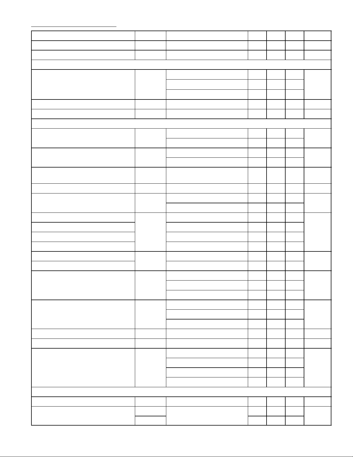
Electrical Characteristics: (TA = +25°C unless otherwise specified)
Parameter Symbol Test Conditions Min Typ Max Unit
Supply Voltage V
Ambient Temperature T
Start Operation (TA = +25°C)
Current Consumption
(V1 Not Yet Switched)
9
A
I
9
V9 = 3.0V – – 0.5 mA
V9 = 5.0V – 1.5 2.0
V9 = 10V – 2.0 3.2
– 15 18 V
–15 – +85 °C
Turn–On Point for V
1
V4 Before Start–Up (V9 < 11.8V) V
V
9
4
11.3 11.8 12.3 V
6.0 6.7 – V
Regulation Mode (V9 = 15V, TA = +25°C)
Current Consumption I
Reference Voltage V
9
V
= –10V 110 135 160 mA
reg
V
= 0 55 85 110
reg
I1 < 0.1mA 4.0 4.2 4.5 V
1
I1 = 5.0mA 4.0 4.2 4.4
Reference Voltage Temperature
TC
1
– 100 – ppm/°C
Coefficient
V
Low Static Voltage V
Pin4
V
Regulation Peak Voltage V
Pin4
V
Full Fold Back V
Pin3
V
Fold Back I
Pin3
V
Overload Decision I
Pin3
V
Regulation – 2.11 –
Pin3
V
Pin3 IPin3
V
Pin3 IPin3
V
Pin7
Regulation I
Leakage V
Peak High V
4
4(peak)IPin3
I
Pin3
I
3
3
7(peak)VR
Pin3
Pin3
Pin3
Pin3
= 5.0µA 4.0 4.2 4.5 V
= 1.3mA – 2.4 3.0
= 1.3mA – 3.7 4.0 V
= 0.5mA – 2.5 3.0
= 1.0µA – 2.4 2.9
= 1.5V – 0.4 –
= 0V (Full Fold Back) – 3.5 – V
1.8 2.08 2.5 V
– 1.0 – µA
VR = –10V (Regulation) – 4.0 –
VR = –15V (Stand–By) – 5.0 –
V
Peak Low V
Pin7
7(peak)VR
= 0V – 1.4 – V
VR = –10V – 1.45 –
VR = –15V – 1.57 –
I
Sink Peak I
Pin7
I
Source Peak I
Pin8
V
Pin2
7(peak)
8(peak)
V
VR = –15V – +0.7 – A
VR = –15V – –0.8 – A
I
2
= –3.0mA – –0.3 – V
Pin2
I
= –0.3mA – –0.2 –
Pin2
I
= +3.0mA – +0.7 –
Pin2
I
= +0.3mA – +0.8 –
Pin2
Protective Operation (V9 = 15V, TA = +25°C)
Current Consumption I
Turn–Off Voltage V
9
V
V5 < 1.8V 14 20 26 mA
V5 < 1.8V 1.3 1.5 1.8 V
7
4
1.8 2.1 2.5
 Loading...