

NTE NTE7001 Datasheet

NTE7001
Integrated Circuit
Horizontal Combination Circuit for
Color TV & Computer Monitors
Description:
The NTE7001 is a monolithic integrated circuit in a 16–Lead DIP type package intended for use in
color television receivers.
Features:
D Horizontal Oscillation Based on the Threshold Switching Principle
D Phase Comparasion Between Sync Pulse and Oscillator Voltage (ϕ
D Internal Key Pulse for Phase Detector (ϕ
) (Additional Noise Limiting)
1
D Phase Comparison Between Line Flyback Pulse and Oscillator Volatge (ϕ
D Larger Catching Range Obtained by Coincidence Detector (ϕ
; Between Sync and Key Pulse)
3
D Switch for Changing the Filter Characteristic and the Gtae Circuit (VCR Operation)
D Sync Separator
D Noise Separator
D Vertical Sync Separator and Output Stage
D Color Burst Keying and Line Flyback Blanking Pulse Generator
D Phase Shifter for the Output Pulse
D Output Pulse Duration Switching
D Output Stage with Separate Supply Voltage for Direct Drive of Thyristor Deflection Circuits
D Low Supply Voltage Protection
)
1
)
2
Applications:
D Video Monitors
D TV Receivers
Absolute Maximum Ratings:
Supply Voltage
at Pin1 (Voltage Source), V
at Pin2, V
2–16
Voltages
Pin4, V
Pin9, ±V
Pin10, ±V
Pin11, V
4–16
9–16
10–16
11–16
1–16
13.2V. . . . . . . . . . . . . . . . . . . . . . . . . . . . . . . . . . . . . . . . . . . . . .
18V. . . . . . . . . . . . . . . . . . . . . . . . . . . . . . . . . . . . . . . . . . . . . . . . . . . . . . . . . . . . . . . .
13.2V. . . . . . . . . . . . . . . . . . . . . . . . . . . . . . . . . . . . . . . . . . . . . . . . . . . . . . . . . . . . . . . .
6V. . . . . . . . . . . . . . . . . . . . . . . . . . . . . . . . . . . . . . . . . . . . . . . . . . . . . . . . . . . . . . . . . .
6V. . . . . . . . . . . . . . . . . . . . . . . . . . . . . . . . . . . . . . . . . . . . . . . . . . . . . . . . . . . . . . . .
13.2V. . . . . . . . . . . . . . . . . . . . . . . . . . . . . . . . . . . . . . . . . . . . . . . . . . . . . . . . . . . . . .
Absolute Maximum Ratings (Cont’d):
Currents
Pin2 and Pin3 (Thyristor Driving, Peak Value), I
Pin2 and Pin3 (Transistor Driving, Peak Value), I
Pin4, I
Pin6, ±I
Pin7, –I
Pin11, I
Total Power Dissipation, P
4
6
7
11
TOT
Operating Ambient Temperature Range, T
Storage Temperature Range, T
stg
2M
2M
, –I
, –I
3M
3M
650mA. . . . . . . . . . . . . . . . . . . . . . . .
400mA. . . . . . . . . . . . . . . . . . . . . . .
1mA. . . . . . . . . . . . . . . . . . . . . . . . . . . . . . . . . . . . . . . . . . . . . . . . . . . . . . . . . . . . . . . . . . . .
10mA. . . . . . . . . . . . . . . . . . . . . . . . . . . . . . . . . . . . . . . . . . . . . . . . . . . . . . . . . . . . . . . . . .
10mA. . . . . . . . . . . . . . . . . . . . . . . . . . . . . . . . . . . . . . . . . . . . . . . . . . . . . . . . . . . . . . . . . .
2mA. . . . . . . . . . . . . . . . . . . . . . . . . . . . . . . . . . . . . . . . . . . . . . . . . . . . . . . . . . . . . . . . . . .
800mW. . . . . . . . . . . . . . . . . . . . . . . . . . . . . . . . . . . . . . . . . . . . . . . . . . . .
A
–20° to +70°C. . . . . . . . . . . . . . . . . . . . . . . . . . . . . . . . . . .
–25°C to +125°C. . . . . . . . . . . . . . . . . . . . . . . . . . . . . . . . . . . . . . . .
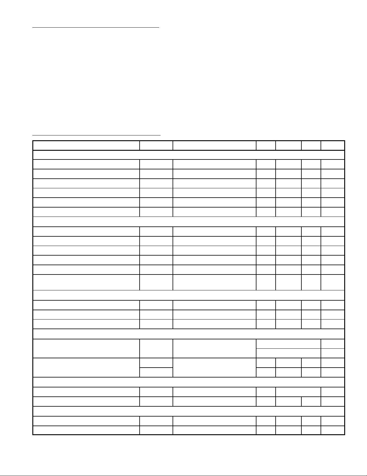
DC and AC Electrical Characteristics:
(VCC = 12V, TA = +25°C unless otherwise specified)
Parameter Symbol Test Conditions Min Typ Max Unit
Sync Separator
Input Switch Voltage V
Input Keying Current I
Input Leakage Current I
Input Switching Current I
Switch OFF Current I
Input Signal (Peak–to–Peak Value) V
9–16
9
9
9
9
9–16(P–P)
V
= –5V – – 1 µA
9–16
Note 1 3 – 4 V
Noise Separator
Input Switching Voltage V
Input Keying Current I
Input Switching Current I
Input Leakage Current I
Input Signal (Peak–to–Peak Value) V
Permissible Superimposed Noise Signal
(Peak–to–Peak Value)
10–16
10
10
10
10–16(P–P)
V
10–16(P–P)
V
= –5V – – 1 µA
10–16
Note 1 3 – 4 V
Line Flyback Pulse
Input Current I
Input Switching Voltage V
Input Limiting Voltage V
6
6–16
6–16
Switching on VCR
Input Voltage V
Input Current –I
11–16
11
I
11
Pulse Duration Switch [t = 7µs (Thyristor Driving)]
Input Voltage V
Input Current I
4–16
4
Pulse Duration Switch [t = 14µs + tD (Transistor Driving)]
Input Voltage V
Input Current –I
4–16
4
– 0.8 – V
5 – 100 µA
– – 5 µA
100 150 – µA
– 1.4 – V
5 – 100 µA
100 150 – µA
– – 7 V
0.02 1 2 mA
– 1.4 – V
–0.7 – +1.4 V
0 to 2.5 V
9 to V
1–16
V
– – 200 µA
– – 2 mA
– 9.4 to V
1–16
V
200 – – µA
0 – 3.5 V
200 – – µA
Note 1. Permissible Range 1V to 7V.
 Loading...