

NTE NTE6889, NTE6880 Datasheet
NTE6880 & NTE6889
Integrated Circuit
Bidirectional Bus Transceiver
Description:
The NTE6880 and NTE6889 consists of 4 pairs of TRI–STA TE logic elements configured as quad bus
drivers/receivers along with separate buffered receiver enable and driver enable lines.
Features:
D TRI–STATE Outputs
Inverting (NTE6880)
Non–Inverting (NTE6889)
D Low Current PNP Inputs: 200µA Max
D Fast Switching Times: 20ns
Absolute Maximum Ratings: (Note 1)
All Outputs and Supply Voltages –0.5V to +7V. . . . . . . . . . . . . . . . . . . . . . . . . . . . . . . . . . . . . . . . . . . . .
All Input Voltages –1V to 5.5V. . . . . . . . . . . . . . . . . . . . . . . . . . . . . . . . . . . . . . . . . . . . . . . . . . . . . . . . . . .
Output Currents ±150mA. . . . . . . . . . . . . . . . . . . . . . . . . . . . . . . . . . . . . . . . . . . . . . . . . . . . . . . . . . . . . . .
Maximum Power Dissipation (TA = +25°C), P
D
1476mW. . . . . . . . . . . . . . . . . . . . . . . . . . . . . . . . . . . .
Derate Above +25°C 11.8mW/°C. . . . . . . . . . . . . . . . . . . . . . . . . . . . . . . . . . . . . . . . . . . . . . . . . . .
Storage Temperature, T
Lead Temperature (Soldering, 4 seconds), T
–65° to +150°C. . . . . . . . . . . . . . . . . . . . . . . . . . . . . . . . . . . . . . . . . . . . . . . .
stg
L
+260°C. . . . . . . . . . . . . . . . . . . . . . . . . . . . . . . . . . . . . . .
Note 1. “Absolute Maximum Ratings” are those values beyons which the safety of the device cannot
be guaranteed. They are not meant to imply that the devices should be operated at these
limits. T he tables of “Electrical Characteristics” provi de conditions for actual device operation.
Recommended Operating Conditions:
Supply Voltage, V
CC
Operating Temperature Range, T
A
4.75 to 5.25V. . . . . . . . . . . . . . . . . . . . . . . . . . . . . . . . . . . . . . . . . . . . . . . . . . . . . . .
0° to +70°C. . . . . . . . . . . . . . . . . . . . . . . . . . . . . . . . . . . . . . . . . . . . .
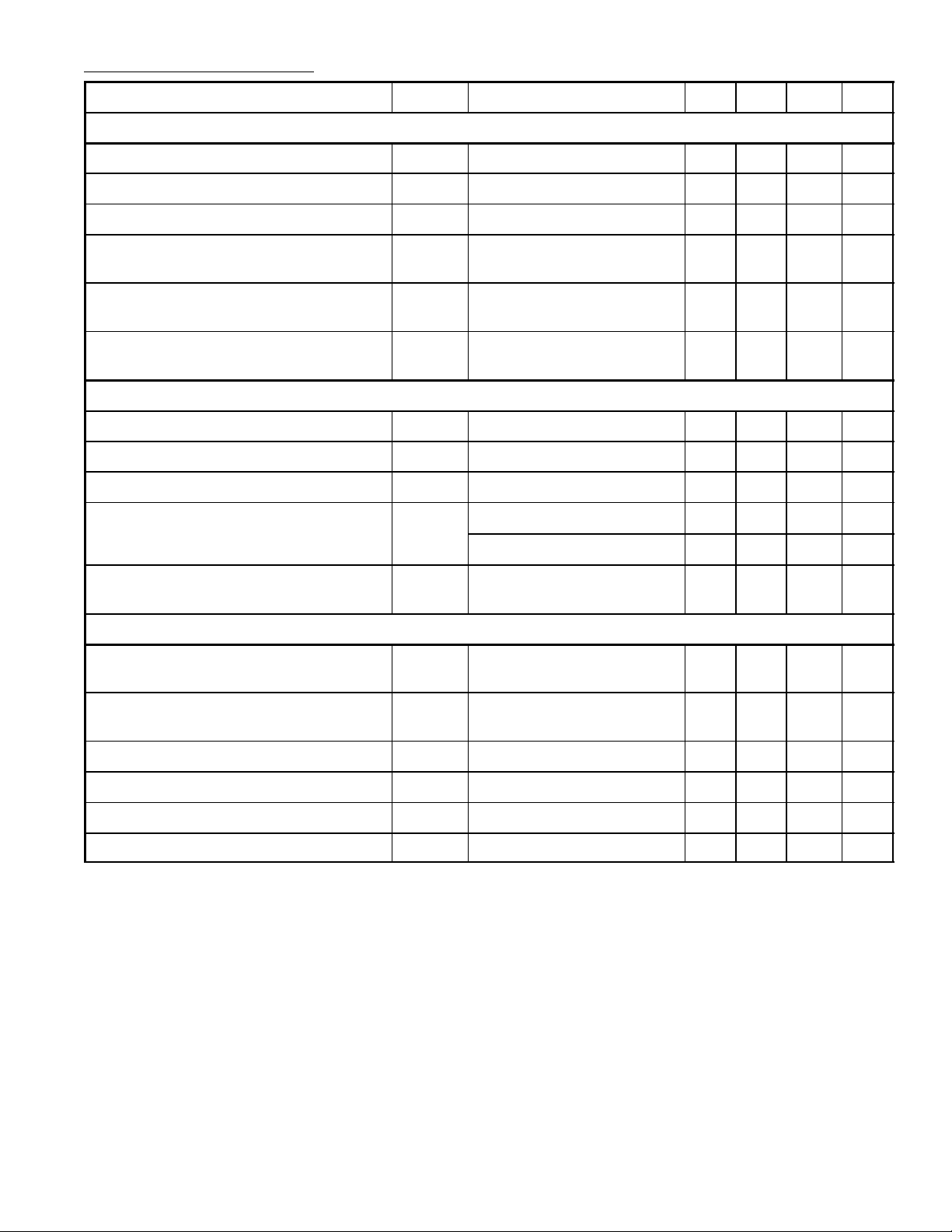
Electrical Characteristics: (TA = 0° to +70°C, Note 2, Note 3 unless otherwise specified)
Parameter Symbol Test Conditions Min Typ Max Unit
DRIVER
Low Level Input Current I
Low Level Input Current (Disabled) I
High Level Input Current (DIN, DE) I
Low Level Output Voltage
(Pin3, Pin6, Pin10, Pin18)
High Level Output Voltage,
V
(Pin3, Pin6, Pin10, Pin13)
Short–Circuit Output Current,
(Pin3, Pin6, Pin10, Pin13)
RECEIVER
Low Level Input Current I
High Level Input Current (RE) I
Low Level Output Voltage V
High Level Output Voltage, V
(Pin2, Pin5, Pin11, Pin14)
Short–Circuit Output Current,
(Pin2, Pin5, Pin11, Pin14)
IL
IL
IH
V
OL
OH
I
OS
IL
IH
OL
OH
I
OB
VIN = 0.4V – – –200 µA
VIN – 0.4V – – –25 µA
VIN =VCC Max – – 25 µA
I
= 48mA – – 0.5 V
OUT
I
= –10mA 2.4 – – V
OUT
V
= 0V, VCC = VCC Max –50 – –150 mA
OUT
VIn = 0.4V – – –200 µA
VIN = VCC Max – – 25 µA
I
= 20mA – – 0.5 V
OUT
I
= –100µA 3.5 – – V
OUT
I
=–2mA 2.5 – – V
OUT
V
= 0V, VCC = VCC Max –30 – –75 mA
OUT
BOTH DRIVER AND RECEIVER
Low Level Input Threshold Voltage V
High Level Input Threshold Voltage V
Low Level Out put OFF Leakage Current I
High Level Output OFF Leakage Current I
Input Clamp Voltage V
Power Supply Current I
TL
TH
OZ
OZ
CC
VCC = Min, VIn = 0.8V,
I
= Max
OL
VCC = Max, VIN = 0.8V,
I
= Max
OH
V
= 0.5V – – –100 µA
OUT
V
= 2.4V – – 100 µA
OUT
IIN = –12mA – – –1.0 V
I
0.85 – – V
– – 2 V
VCC = VCC Max – – 110 mA
Note 2. All currents into device pins are positive, all currents out of device pins are negative. All volt-
ages are referenced to GND unless otherwise specified.
Note 3. Only one output at a time should be shorted.
 Loading...