


NTE6860
Integrated Circuit
NMOS – FSK Digital Modem, 600bps
Description:
The NTE6860 is a MOS subsystem in a 24–Lead DIP type plastic package designed to be integrated
into a wide range of equipment utilizing serial data communications.
The modem provides the necessary modulation, demodulation and supervisory control functions to
implement a serial data communications link, over a voice grade channel, utilizing frequency shift keying (FSK) at bit rates up to 600 bps. The NTE6860 can be implemented into a wide range of data
handling systems, including stand alone modems, data storage devices, remote data communication
terminals and I/O interfaces for minicomputers.
N–channel silicon–gate technology permits the NTE6860 to operate using a single–voltage supply
and be fully TTL compatible.
The modem is compatible with the NTE6860 microcomputer family, interfacing directly with the
Asynchronous Communications Interface Adapter to provide low–speed data communications capability.
Features:
D Originate and Answer Mode
D Crystal or External Reference Control
D Modem Self Test
D Terminal Interfaces TTL–Compatible
D Full–Duplex or Half–Duplex Operation
D Automatic Answer and Disconnect
D Compatible Functions for 100 Series Data Sets
D Compatible Functions for 1001A/B Data Couplers
Absolute Maximum Ratings:
Supply Voltage, VCC –0.3 to +7.0V. . . . . . . . . . . . . . . . . . . . . . . . . . . . . . . . . . . . . . . . . . . . . . . . . . . . . .
Input Voltage, Vin –0.3 to +7.0V. . . . . . . . . . . . . . . . . . . . . . . . . . . . . . . . . . . . . . . . . . . . . . . . . . . . . . . . .
Operating Temperature Range, TA 0° to 70°C. . . . . . . . . . . . . . . . . . . . . . . . . . . . . . . . . . . . . . . . . . . . .
Storage Temperature Range, T
Thermal Resistance, Junction–to–Ambient, R
Note 1. This device contains circuitry to protect the inputs against damage due to high static voltages
or electric fields; however, it is advised that normal precautions be taken to avoid application
of any voltage higher than maximum rated voltages to this high impedance circuit.
Reliability of operation is enhanced if unused inputs are tied to an appropriate logic voltage
level (e.g. either VSS or VCC).
–55° to +150°C. . . . . . . . . . . . . . . . . . . . . . . . . . . . . . . . . . . . . . . . . .
stg
thJA
+120°C/W. . . . . . . . . . . . . . . . . . . . . . . . . . . . . . . . .
Power Considerations:
The average chip–junction temperature, TJ, in °C can be obtained from:
1. TJ = TA + (PD R
)
Θ
JA
Where:
T
A
R
P
P
P
For most applications P
5 Ambient Temperature, °C
5 Package Thermal Resistance, Junction to Ambient, °C/W
Θ
JA
5 P
D
5 iCC x VCC, Watts – Chip Internal Power
INT
5 Port Power Dissipation, Watts – User Determined
PORT
INT
PORT
+ P
Ơ P
PORT
and can be neglected. P
INT
may become significant if the de-
PORT
vice is configured to drive Darlington bases or sink LED loads.
An approximate relationship between PD and TJ (if P
is neglected) is:
PORT
2. PD = K B (TJ + 273°C)
Solving equations 1 and 2 for K gives:
3. K = PD (TA + 273°C) + R
Θ
JA
P
2
D
Where K is a constant pertaining to the particular part. K can be determined from equation 3 by measuring PD (at equilibrium) for a known TA. Using this value of K the values of PD and TJ can be obtained
by solving equations 1 and 2 iteratively for any value of TA.
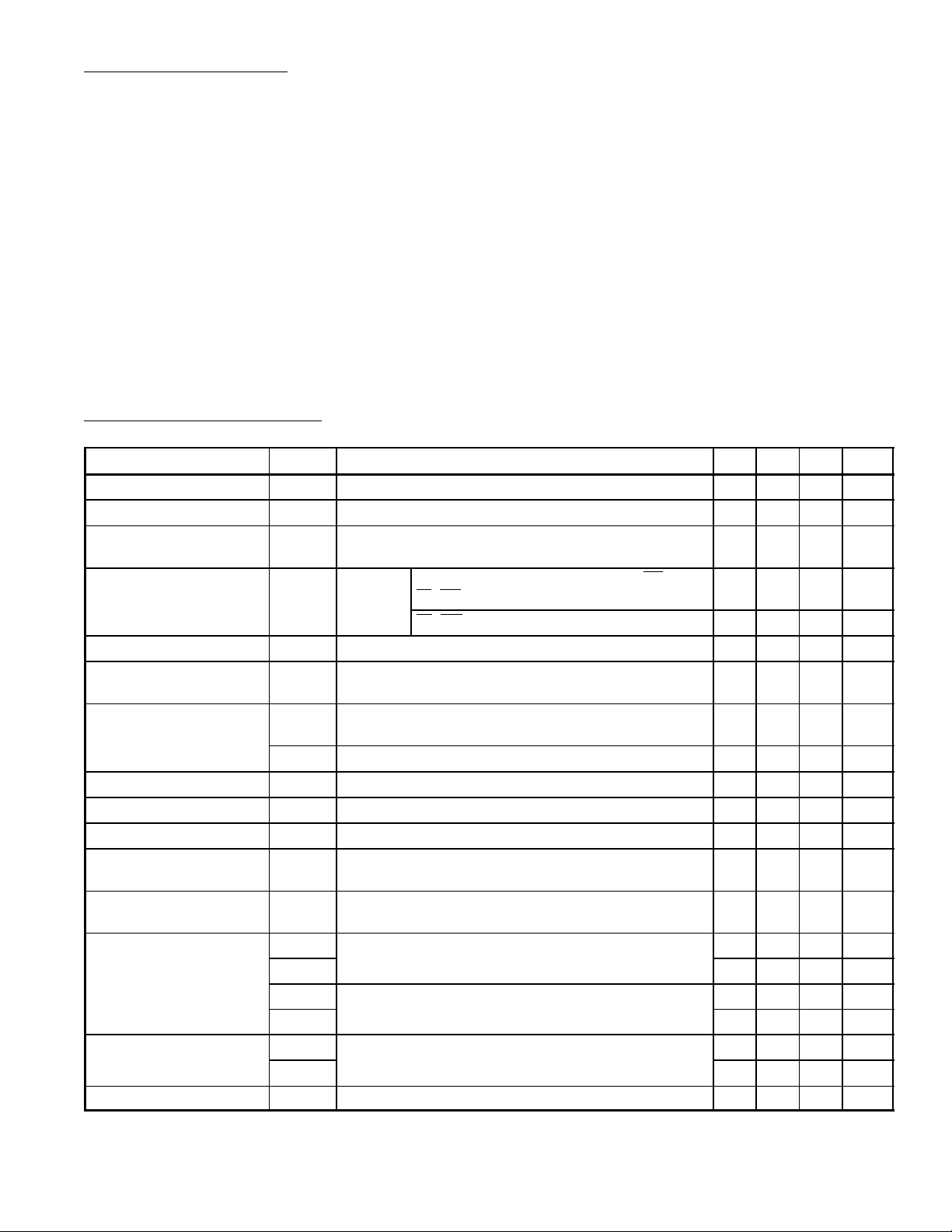
DC Electrical Characteristics:(VCC = 5V ±5%, all voltages referenced to VSS = 0, TA = 0° to +70°C
unless otherwise specified)
Parameter Symbol Test Conditions Min Typ Max Unit
Input High Voltage V
Input Low Voltage V
Crystal Input Voltage V
Input Current I
Input Leakage Current I
Output High Voltage V
Output Low Voltage V
V
Output High Current I
Input Capacitance C
Output Capacitance C
Transmit Carrier Output
V
Voltage
Transmit Carrier Output
V
2nd Harmonic
Input Transition Times t
Output Transistion Times t
Internal Power Dissipation P
IH
IL
in
in
IL
OH1
OL1
OL2
OH2
in
out
CO
2H
r
t
f
t
r
t
f
r
t
f
INT
All Inputs Except Crystal 2.0 – V
All Inputs Except Crystal V
Crystal Input D riven from an External Reference, Input
1.5 – 2.0 V
– 0.80 V
SS
CC
V
P–P
Coupling Capacitor = 200pF, Duty Cycle = 50 ±5%
Vin = VSSAll Inputs Except Rx Car, Tx Data, TD, TST,
– – –0.2 mA
RI, SH
RI, SH Inputs – – –1.6 mA
Vin = 7V, VCC = VSS, TA = +25°C – – 1.0 µA
All Outputs Except An Ph and Tx Car, I
= –0.04mA,
OH1
2.4 – V
CC
V
Load A
All Outputs Except An Ph and Tx Car, I
= 1.6mA,
OL1
V
– 0.40 V
SS
Load A
An Ph, I
An Ph, V
= 0, Load B V
OL2
= 0.8V, Load B 0.30 – – mA
OH2
– 0.30 V
SS
f = 0.1Mhz, TA = +25°C – 5.0 – pF
f = 0.1Mhz, TA = +25°C – 10 – pF
Load C 0.20 0.35 0.50 V
RMS
Load C –25 –32 – dB
All Inputs Except Crystal, Operating in the Crystal Input
Mode; from 10% to 90% Points, Note 2
Ctystal Input, Operating in External Input Reference
Mode
– – 1.0 µs
– – 1.0 µs
– – 30 µs
– – 30 µs
All Outputs Except Tx Car, From 10% to 90% Points – – 5.0 µs
– – 5.0 µs
All Inputs at VSS and All Outputs Open, TA = 0°C – – 340 mW
Note 2. Maximum Input Transition Times are ≤ 0.1 x Pulse Width or the specified maximum of 1µs,
whichever is smaller.
 Loading...