

NTE NTE6810 Datasheet

NTE6810
Integrated Circuit
128 x 8–Bit Static Random Access Memory (SRAM)
Description:
The NTE6810 is a byte–orgainzed memory in a 24–Lead DIP type package designed for use in bus–
organized systems. It is fabricated with N–channel silicon–gate technology. For ease of use, this
device operates from a single power supply, has compatibility with TTL and DTL, and needs no clocks
or refreshing because of static operation.
The memory is compatible with the 6800 Microcomputer Family, providing random storage in byte
increments. Memory expansion is provided through multiple Chip Select inputs.
Features:
D Organized as 128 Bytes of 8–Bits
D Static Operation
D Bidirectional Three–State Data Input/Output
D Six Chip Select Inputs (Four Active Low, Two Active High)
D Single 5V Power Supply
D TTL Compatible
D Maximum Access Time: 450ns
Absolute Maximum Ratings:
Supply Voltage, V
Input Voltage, V
Operating Temperature Range, T
Storage Temperature Range, T
CC
in
A
stg
Thermal Resistance, Junction to Ambient, R
Θ
JA
–0.3 to +7V. . . . . . . . . . . . . . . . . . . . . . . . . . . . . . . . . . . . . . . . . . . . . . . . . . . . . . . . .
–0.3 to +7V. . . . . . . . . . . . . . . . . . . . . . . . . . . . . . . . . . . . . . . . . . . . . . . . . . . . . . . . . . . .
0° to +70°C. . . . . . . . . . . . . . . . . . . . . . . . . . . . . . . . . . . . . . . . . . . . .
–65° to +150°C. . . . . . . . . . . . . . . . . . . . . . . . . . . . . . . . . . . . . . . . . .
+120°C/W. . . . . . . . . . . . . . . . . . . . . . . . . . . . . . . . . .
Note 1. This device contains circuitry to protect the inputs against damage due to high static voltages
or electric fields; however, it is advised that normal precautions be taken to avoid application
of any voltage higher than maximum rated voltages to this high impedance circuit. Reliability
of operation is enhanced if unused inputs are tied to an appropriate logic voltage (e.g., either
VSS or VCC).
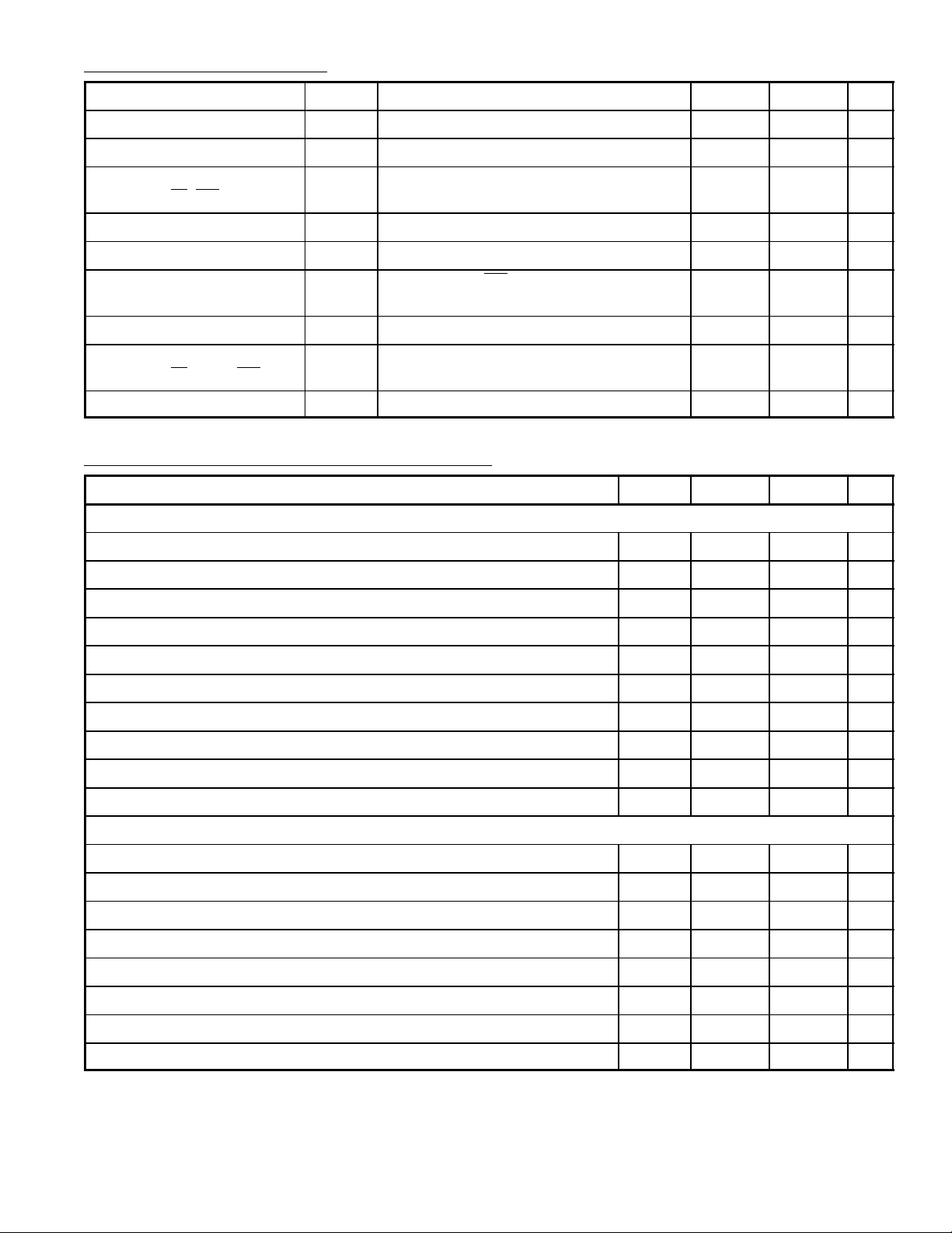
DC Electrical Characteristics: (VCC = 5V ±5%, VSS = 0, TA = 0° to +70°C unless otherwise specified)
Parameter Symbol Test Conditions Min Max Unit
Input High Voltage V
Input Low Voltage V
Input Current
(A
, R/W, CSn)
n
Output High Voltage V
Output Low Voltage V
Output Leakage Current
(Three–State)
Supply Current I
Input Capacitance
(A
, R/W, CSn, CSn)
n
Output Capacitance (Dn) C
I
C
IH
IL
I
in
OH
OL
TSI
CC
in
out
Vin = 0 to 5.25V – 2.5 µA
IOH = –205µA 2.4 – V
IOL = 1.6mA – 0.4 V
CS = 0. 8V or CS = 2V,
V
= 0.4V to 2.4V
out
VCC = 5.25V, All other pins grounded – 80 mA
Vin = 0, TA = +25°C, f = 1MHz – 7.5 pF
V
= 0, TA = +25°C, f = 1MHz, CSO = 0 – 12.5 pF
out
AC Operating Conditions and Characteristics:
Parameter Symbol Min Max Unit
Read Cycle (VCC = 5V ±5%, VSS = 0, TA = 0° to +70° unless otherwise specified)
Read Cycle Time t
Access Time t
Address Setup Time t
Address Hold Time t
Data Delay Time (Read) t
Read to Select Delay Time t
Data Hold from Address t
Output Hold Time t
Data Hold from Read t
Read Hold from Chip Select t
Write Cycle (VCC = 5V ±5%, VSS = 0, TA = 0° to +70° unless otherwise specified)
cyc(R)
acc
AS
AH
DDR
RCS
DHA
H
DHR
RH
VSS +2.0 V
CC
VSS –0.3 VSS +0.8 V
– 10 µA
450 – ns
– 450 ns
20 – ns
0 – ns
– 230 ns
0 – ns
10 – ns
10 – ns
10 80 ns
0 – ns
V
Write Cycle Time t
cyc(W)
Address Setup Time t
Address Hold Time t
Chip Select Pulse Width t
Write to Chip Select Delay Time t
Data Setup Time (Write) t
Input Hold Time t
Write Hold Time from Chip Select t
AS
AH
CS
WCS
DSW
H
WH
450 – ns
20 – ns
0 – ns
300 – ns
0 – ns
190 – ns
10 – ns
0 – ns
 Loading...