

NTE NTE6809E, NTE6809 Datasheet
NTE6809 & NTE6809E
Integrated Circuit
NMOS, 8–Bit Microprocessor (MPU)
Description:
The NTE6809 and NTE6809E are revolutionary high performance 8–bit microprocessors in 40–Lead
DIP type packages which support modern programming techniques such as position independece,
reentrancy, and modular programming.
The basic instructions of any computer are greatly enhanced by the presence of powerful addressing
modes. The NTE6809 and NTE6809E have the most complete set of addressing modes available
on any 8–bit microprocessor today.
These devices contain hardware and software features which make them ideal processors for higher
level language execution or standard controller applications. External clock inputs are provided on
the NTE6809E to allow synchronization with peripherals, systems, or other MPUs.
Architectural Features:
D Two 16–Bit Index Registers
D Two 16–Bit Indexable Stack Pointers
D Two 8–Bit Accumulators can be Concatenated to Form One 16–Bit Accumulator
D Direct Page Register Allows Direct Addressing Throughout Memory
Hardware Features:
D On–Chip Oscillator (Crystal Frequency = 4 x E), NTE6809 Only
D DMA/BREQ
D External Clock Inputs, E and Q, Allow Synchronization, NTE6809E Only
D TSC Input Controls Internal Bus Buffers, NTE6809E Only
D LIC Indicates Opcode Fetch, NTE6809E Only
D AVMA Allows Efficient Use of Common Resource in a Multiprocessor System, NTE6809E Only
D BUSY is a Status Line for Multiprocessing, NTE6809E Only
D Fast Interrupt Request Input Stacks Only Condition Code Register and Program Counter
D MRDY Input Extends Data Across Times for Use with Slow Memory
D Interrupt Acknowledge Output Allows Vectoring by Devices
D Sync Acknowledge Output Allows for Synchronization to External Event
D Single Bus–Cycle RESET
D Single 5V Supply Operation
D NMI
D Early Address Valid Allows Use with Slower Memories
D Early Write Data for Dynamic Memories
Inhibited After RESET Until After First Load Stack Pointer
Allows DMA Operation on Memory Refresh, NTE6809 Only
Software Features:
D 10 Addressing Modes
S M6800 Upward Compatible Addressing Modes
S Direct Addressing Anywhere in Memory Map
S Long RelativeBranches
S Program Counter Relative
S True Indirect Addressing
S Expanded Indexed Addressing
0–, 5–, 8–, or 16–Bit Constant Offsets
8– or 16–Bit Accumulator Offsets
Auto–Increment/Decrement by 1 or 2
D Improved Stack Manipulation
D 1464 Instruction with Unique Addressing Modes
D 8 x 8 Unsigned Multiply
D 16–Bit Arithmetic
D Transfer/Exchange All Registers
D Push/Pull Any Registers or Any Set of Registers
D Load Effective Address
Absolute Maximum Ratings:
Supply Voltage, V
Input Voltage, V
CC
in
Operating Ambient Temperature Range, T
Storage Temperature Range, T
Thermal Resistance, Junction–to–Ambient, R
(Note 1)
stg
–0.3 to +7.0V. . . . . . . . . . . . . . . . . . . . . . . . . . . . . . . . . . . . . . . . . . . . . . . . . . . . . . .
–0.3 to +7.0V. . . . . . . . . . . . . . . . . . . . . . . . . . . . . . . . . . . . . . . . . . . . . . . . . . . . . . . . . .
A
0° to +70°C. . . . . . . . . . . . . . . . . . . . . . . . . . . . . . . . . . . . .
–55° to +150°C. . . . . . . . . . . . . . . . . . . . . . . . . . . . . . . . . . . . . . . . . .
thJA
100°C/W. . . . . . . . . . . . . . . . . . . . . . . . . . . . . . . . . .
Note 1. These devices contain circuitry to protect the inputs against damage due to high static volt-
ages or electric fields; however, it is advised that normal precautions be taken to avoid application of any voltage higher than maximum rated voltages to these high impedance circuits. Reliability of operation is enhanced if unused inputs are tied to an appropriate logic
IH
V
IHR
IHC
IL
ILC
V
ILQ
in
or VCC).
SS
VSS+2.0 – V
VSS+4.0 – V
VCC–0.75 – VCC+0.3 V
VSS–0.3 – VSS+0.8 V
VSS–0.3 – VSS+0.4 V
VSS–0.3 – VSS+0.6 V
Vin = 0 to 5.25V, VCC = Max – – 2.5 µA
CC
CC
V
V
voltage level (e.g., either V
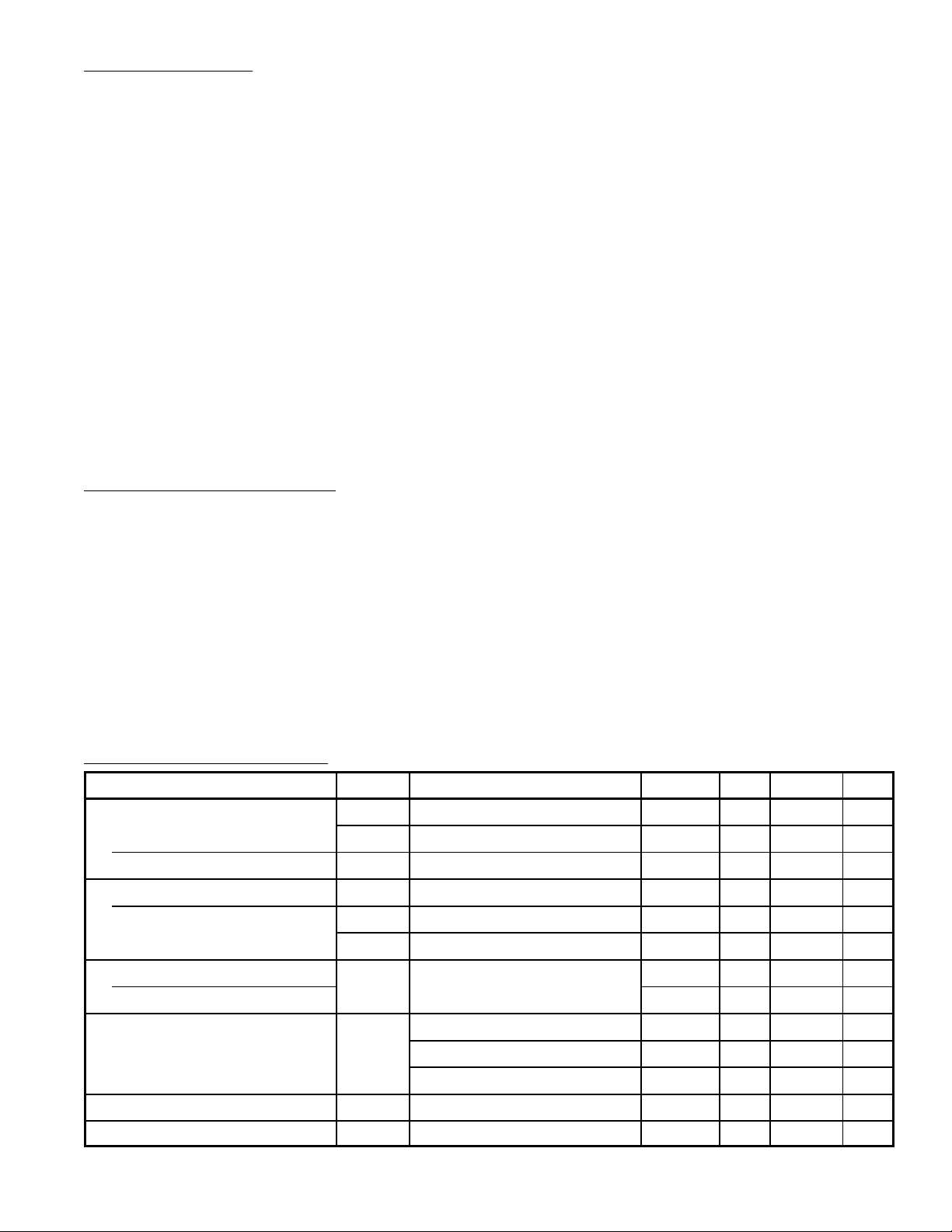
DC Electrical Characteristics:
Parameter Symbol Test Conditions Min Typ Max Unit
Input High Voltage V
NTE6809E Only V
Input Low Voltage V
NTE6809E Only V
Input Leakage Current I
NTE6809E Only (E) – – 100 µA
(VCC = 5V ±5%, VSS = 0, TA = 0° to +70°C unless otherwise specified)
DC Output High Voltage V
DC Output Low Voltage V
Internal Power Dissipation P
OH
OL
INT
I
= 145µA, VCC = Min VSS +2.4 – – V
Load
I
= 205µA, VCC = Min VSS+2.4 – – V
Load
I
= 100µA, VCC = Max VSS+2.4 – – V
Load
I
= 2mA, VCC = Min – – VSS+0.5 V
Load
TA = 0°, Steady State Operation – – 1.0 W
 Loading...