

NTE NTE68, NTE388 Datasheet

NTE388 (NPN) & NTE68 (PNP)
Silicon Complementary Transistors
General Purpose High Power Audio,
Disk Head Positioner for Linear Applications
Description:
The NTE388 (NPN) and NTE68 (PNP) are complementary silicon power transistors in a TO3 type
package designed for high power audio, disk head positioners, and other linear applications.
Features:
D High Safe Operating Area: 2A @ 80V
D High DC Current Gain: h
Absolute Maximum Ratings:
Collector–Emitter Voltage, V
Collector–Emitter Voltage, V
Collector–Base Voltage, V
Emitter–Base Voltage, V
Collector Current, I
EBO
C
Continuous 16A. . . . . . . . . . . . . . . . . . . . . . . . . . . . . . . . . . . . . . . . . . . . . . . . . . . . . . . . . . . . . . . . . .
Peak (Note 2) 30A. . . . . . . . . . . . . . . . . . . . . . . . . . . . . . . . . . . . . . . . . . . . . . . . . . . . . . . . . . . . . . . .
Continuous Base Current, I
Total Power Dissipation (T
Derate Above 25°C 1.43W/°C. . . . . . . . . . . . . . . . . . . . . . . . . . . . . . . . . . . . . . . . . . . . . . . . . . . . . .
Operating Junction Temperature Range, T
Storage Temperature Range, T
Thermal Resistance, Junction–to–Case, R
= 15 Min @ IC = 8A
FE
CEO
CEX
CBO
B
= +25°C), P
C
stg
D
J
thJC
250V. . . . . . . . . . . . . . . . . . . . . . . . . . . . . . . . . . . . . . . . . . . . . . . . . . . . .
400V. . . . . . . . . . . . . . . . . . . . . . . . . . . . . . . . . . . . . . . . . . . . . . . . . . . . .
400V. . . . . . . . . . . . . . . . . . . . . . . . . . . . . . . . . . . . . . . . . . . . . . . . . . . . . .
5V. . . . . . . . . . . . . . . . . . . . . . . . . . . . . . . . . . . . . . . . . . . . . . . . . . . . . . . . . .
5A. . . . . . . . . . . . . . . . . . . . . . . . . . . . . . . . . . . . . . . . . . . . . . . . . . . . . . . . . .
250W. . . . . . . . . . . . . . . . . . . . . . . . . . . . . . . . . . . . . . . . . . .
–65° to +200°C. . . . . . . . . . . . . . . . . . . . . . . . . . . . . . . . . .
–65° to +200°C. . . . . . . . . . . . . . . . . . . . . . . . . . . . . . . . . . . . . . . . . .
0.70°C/W. . . . . . . . . . . . . . . . . . . . . . . . . . . . . . . . . . . .
Note 1. Matched complementary pairs are available upon request (NTE68MCP). Matched comple-
mentary pairs have their gain specification (h
) matched to within 10% of each other.
FE
Note 2. Pulse Test: Pulse Width = 5ms, Duty Cycle ≤ 10%.
Electrical Characteristics: (TC = +25°C unless otherwise specified)
Parameter Symbol Test Conditions Min Typ Max Unit
OFF Characteristics
Collector–Emitter Sustaining Voltage V
Collector Cutoff Current I
Emitter Cutoff Current I
CEO(sus)IC
CEX
I
CEO
EBO
= 100mA, IB = 0, Note 3 250 – – V
VCE = 250V, V
= 1.5V – – 250 µA
BE(off)
VCE = 200V, IB = 0 – – 500 µA
VEB = 5V, IC = 0 – – 500 µA
Second Breakdown
Second Breakdown Collector Current
with Base Forward Bias
I
S/b
VCE = 50V, t = 0.5s (non–repetitive) 5 – – µA
VCE = 80V, t = 0.5s (non–repetitive) 2 – – µA
ON Characteristics
DC Current Gain h
FE
VCE = 4V, IC = 8A 15 – 60
VCE = 4V, IC = 16A 5 – –
Collector–Emitter Saturation Voltage V
CE(sat)IC
= 8A, IB = 800mA – – 1.4 V
IC = 16A, IB = 3.2A – – 4.0 V
Base–Emitter On Voltage V
BE(on)
VCE = 4V, IC = 8A
Dynamic Characteristics
Current Gain–Bandwidth Product f
Output Capacitance C
VCE = 10V, IC = 1A, f
T
VCB = 10V, IE = 0, f
ob
test
test
Note 3. Pulse Test: Pulse Width = 300µs, Duty Cycle ≤ 2%.
–
– 2.2 V
= 1MHz 4 – – MHz
= 1MHz – – 500 pF
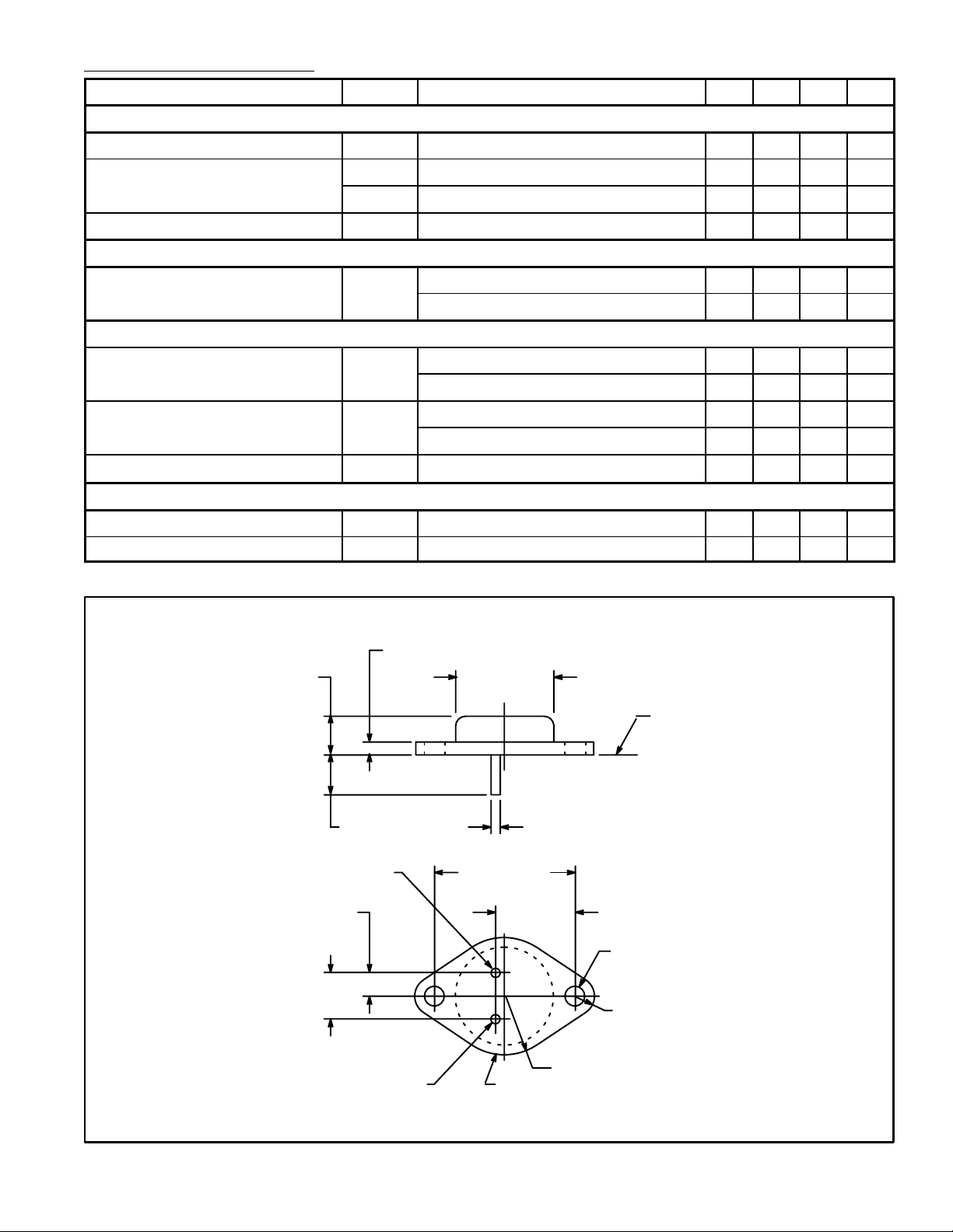
.350 (8.89)
.215 (5.45)
Emitter
.430
(10.92)
.135 (3.45) Max
.875 (22.2)
Dia Max
Seating
Plane
.040 (1.02).312 (7.93) Min
1.187
(30.16)
.665
(16.9)
.156 (3.96) Dia
(2 Holes)
.188 (4.8) R Max
.525 (13.35) R Max
Collector/CaseBase
 Loading...