

NTE NTE6508 Datasheet
NTE6508
Integrated Circuit
CMOS, 1K Static RAM (SRAM)
Description:
The NTE6508 is a 1024 x 1 fully static CMOS RAM in a 16–Lead DIP type package fabricated using
self–aligned silicon gate technology. Synchronous circuit design techniques are employed to acheive
high performance and low power operation. On chip latches are provided for address allowing effecient interfacing with microprocessor systems. The data output buffers can be forced to a high impedance state for use in expanded memory arrays.
Features:
D Low Power Standby: 50µW Max
D Low Power Operation: 20mW/MHz Max
D Fast Access Time: 300ns Max
D Data Retention: 2V Min
D TTL Compatible Input/Output
D High Output Drive: 2 TTL Loads
D On–Chip Address Register
Absolute Maximum Ratings:
Supply Voltage +7V. . . . . . . . . . . . . . . . . . . . . . . . . . . . . . . . . . . . . . . . . . . . . . . . . . . . . . . . . . . . . . . . . . . . .
Input, Output or I/O Voltage GND –0.3V to V
Typical Derating Factor 1.5mA/MHz increase in I
Gate Count 1925 Gates. . . . . . . . . . . . . . . . . . . . . . . . . . . . . . . . . . . . . . . . . . . . . . . . . . . . . . . . . . . . . . . . .
Operating Junction Temperature +175°C. . . . . . . . . . . . . . . . . . . . . . . . . . . . . . . . . . . . . . . . . . . . . . . . . .
Storage Temperature Range –65° to +150°C. . . . . . . . . . . . . . . . . . . . . . . . . . . . . . . . . . . . . . . . . . . . . . .
Lead Temperature (During Soldering, 10s max) +300°C. . . . . . . . . . . . . . . . . . . . . . . . . . . . . . . . . . . . .
Note 1. Stresses above those listed in “Absolute Maximum Ratings” may cause permanent damage
to the device. This is a stress only rating and operation of the device at these or any other
conditions above those indicated in the operational sections of this specification is not implied. This device is sensitive to electrostatic discharge, users should follow proper IC handling procedures.
Recommended Operating Conditions:
Operating Voltage Range +4.5V to +5.5V. . . . . . . . . . . . . . . . . . . . . . . . . . . . . . . . . . . . . . . . . . . . . . . . . .
Operating Temperature Range –40° to +85°C. . . . . . . . . . . . . . . . . . . . . . . . . . . . . . . . . . . . . . . . . . . . . .
(Note 1)
. . . . . . . . . . . . . . . . . . . . . . . . . . . . . . . . . . . . .
CC
+0.3V. . . . . . . . . . . . . . . . . . . . . . . . . . . . . . . . . . . . . . .
CC(OP)
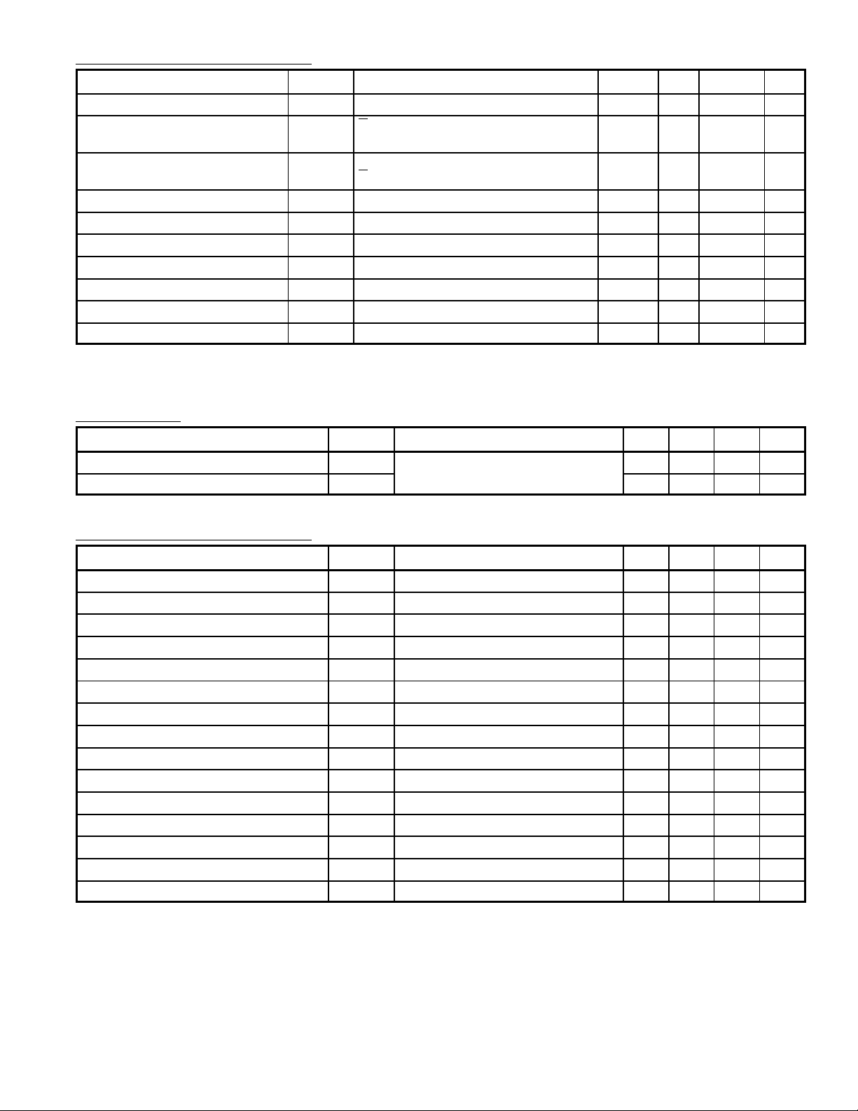
DC Electrical Characteristics: VCC = 5V ±10%, TA = –40° to +85°C unless otherwise specified)
Parameter Symbol Test Conditions Min Typ Max Unit
Standby Supply Current I
Operating Supply Current I
Data Retention Supply Current I
Data Retention Supply Voltage V
CC(SB)IO
CC(OP)
CC(DR)VCC
CC(DR)
Input Leakage Current I
Output Leakage Current I
Input Voltage, LOW V
Input Voltage, HIGH V
Output Voltage, LOW V
Output Voltage, HIGH V
I
OZ
IL
IH
OL
OH
= 0, VI = VCC or GND, VCC = 5V – – 10 µA
E = 1MHz, IO = 0, VI = VCC or GND,
= 5.5V, Note 2
V
CC
= 2V, IO = 0, VI = VCC or GND,
= V
E
CC
– – 4 mA
– – 10 µA
2.0 – – V
VI = VCC or GND, VCC = 5.5V –1.0 – +1.0 µA
VO = VCC or GND, VCC = 5.5V –1.0 – +1.0 µA
VCC = 4.5V –0.3 – +0.8 V
VCC = 5.5V VCC–2 – VCC+0.3 V
IO = 3.2mA, VCC = 4.5V – – 0.4 V
IO = –0.4mA, VCC = 4.5V 2.4 – – V
Note 2. Typical derating 1.5mA/MHz increase in I
Capacitance:
(TA = +25°C unless otherwise specified)
CC(OP)
.
Parameter Symbol Test Conditions Min Typ Max Unit
Input Capacitance C
Output Capacitance C
f = 1MHz, All measurements are ref-
I
erenced to device GND
O
– – 6 pF
– – 10 pF
AC Electrical Characteristics: VCC = 5V ±10%, TA = –40° to +85°C unless otherwise specified)
Parameter Symbol Test Conditions Min Typ Max Unit
Chip Enable Access Time TELQV Note 3, Note 5 – – 300 ns
Address Access Time TAVQV Note 3, Note 5, & Note 6 – – 300 ns
Chip Enable Output Enable Time TELQX Note 4, Note 5 5 – 160 ns
Write Enable Output Disable Time TWLQZ Note 4, Note 5 – – 160 ns
Chip Enable Output Disable Time TEHQZ Note 4, Note 5 – – 160 ns
Chip Enable Pulse Negative Width TELEH Note 3, Note 5 300 – – ns
Chip Enable Pulse Positive Width TEHEL Note 3, Note 5 100 – – ns
Address Setup Time TAVEL Note 3, Note 5 0 – – ns
Address Hold Time TELAX Note 3, Note 5 50 – – ns
Data Setup Time TDVWH Note 3, Note 5 110 – – ns
Data Hold Time TWHDX Note 3, Note 5 0 – – ns
Chip Enable Write Pulse Setup Time TWLEH Note 3, Note 5 130 – – ns
Chip Enable Write Pulse Hold Time TELWH Note 3, Note 5 130 – – ns
Write Enable Pulse Width TWLWH Note 3, Note 5 130 – – ns
Read or Write Cycle Time TELEL Note 3, Note 5 350 – – ns
Note 3. Input pulse levels: 0.8V to VCC –2V; Input rise and fall times: 5ns (max); Input and output
timing reference level: 1.5V; Output load: 1 TTL gate equivalent, CL = 50pF (min) – for C
greater than 50pF, access time is derated by 0.15ns per pF.
Note 4. Tested at initial design and after major design changes.
Note 5. V
= 4.5V and 5.5V.
CC
Note 6. TAVQV = TELQV + TAVEL.
L
 Loading...