

NTE NTE6410 Datasheet
NTE6410
Unijunction Transistor (UJT)
Description:
The NTE6410 is a PN unijunction transistor in a TO92 type package designed for use in pulse and
timing circuits, sensing circuits and thyristor trigger circuits.
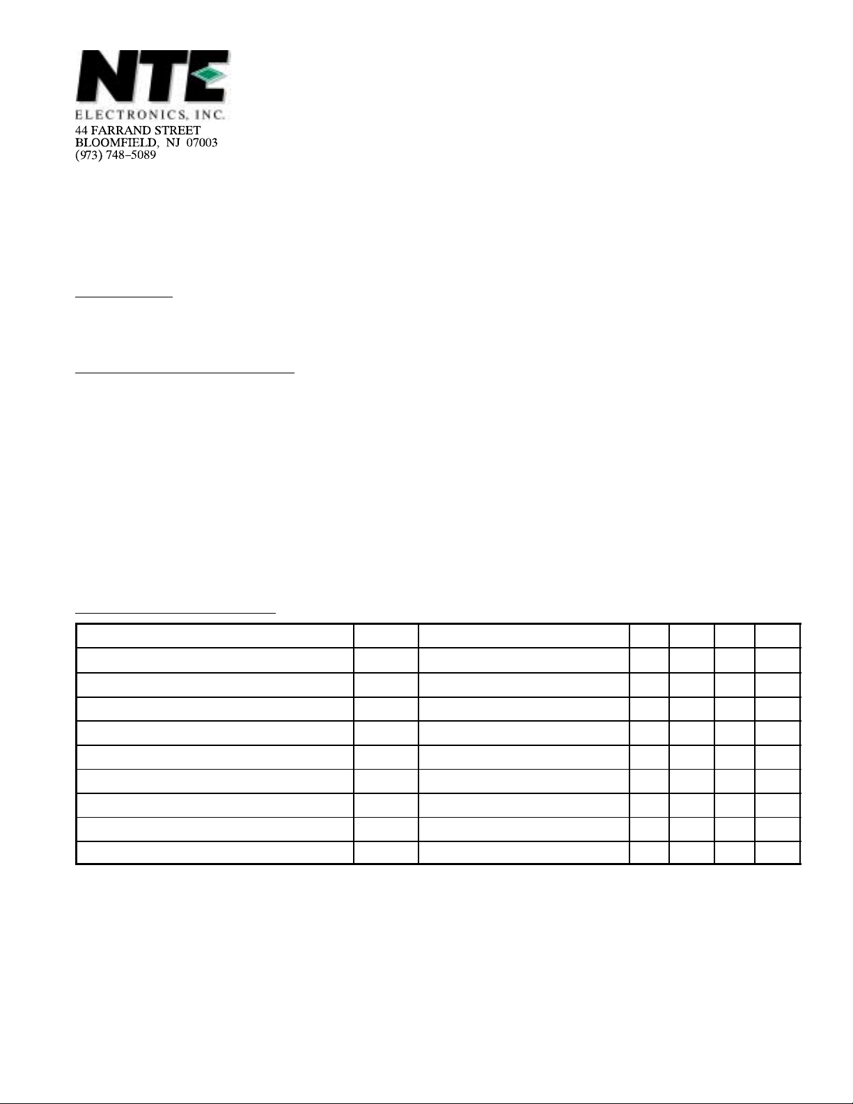
Absolute Maximum Ratings: (TA = +25°C unless other specified)
RMS Power Dissipation, P
D
Derate Above 25°C 3.0mW/°C. . . . . . . . . . . . . . . . . . . . . . . . . . . . . . . . . . . . . . . . . . . . . . . . . . . . .
RMS Emitter Current, I
Peak–Pulse Emitter Current (Note 1), I
Emitter Reverse Voltage, V
Interbase Voltage (Note 2), V
E
E
B2E
B2B1
Operating Junction Temperature Range, TJ –65° to +125°C. . . . . . . . . . . . . . . . . . . . . . . . . . . . . . . . .
Storage Temperature Range, T
–65° to +150°C. . . . . . . . . . . . . . . . . . . . . . . . . . . . . . . . . . . . . . . . . .
stg
Note 1. Duty cycle ≤ 1%, PRR = 10 PPS
Note 2. Based upon power dissipation at TA = +25°C
Electrical Characteristics: (TA = +25°C unless other specified)
Parameter Symbol Test Conditions Min Typ Max Unit
300mW. . . . . . . . . . . . . . . . . . . . . . . . . . . . . . . . . . . . . . . . . . . . . . . . . . . . . .
50mA. . . . . . . . . . . . . . . . . . . . . . . . . . . . . . . . . . . . . . . . . . . . . . . . . . . . . . . . . . .
1.5A. . . . . . . . . . . . . . . . . . . . . . . . . . . . . . . . . . . . . . . . . . . . . .
30V. . . . . . . . . . . . . . . . . . . . . . . . . . . . . . . . . . . . . . . . . . . . . . . . . . . . . . .
35V. . . . . . . . . . . . . . . . . . . . . . . . . . . . . . . . . . . . . . . . . . . . . . . . . . . .
Intrinsic Standoff Ratio
Interbase Resistance R
Interbase Resistance Temperature Coefficient αR
Emitter Saturation Voltage V
Modulated Interbase Current I
Emitter Reverse Current I
Peak–Point Emitter Current I
Valley–Point Current I
Base–One Peak Pulse Voltage V
BE1(sat)VB2B1
B2(Mod)VB2B1
EB2O
η
OB1
BB
P
V
BB
V
= 10V, Note 3 0.70 – 0.85
B2B1
4.0 6.0 9.1 kΩ
0.1 – 0.9 %/°C
= 10V, IE = 50mA, Note 4 – 2.5 – V
= 10V, IE = 50mA – 15 – mA
V
= 30V, IB1 = 0 – 0.005 1.0 µA
B2E
V
= 25V – 1.0 5.0 µA
B2B1
V
= 20V, RB2 = 100Ω, Note 4 4.0 7.0 – mA
B2B1
5.0 8.0 – V
Note 3. Intrinsic standoff ratio, is defined in terms of peak–point voltage, VP, by means of the equa-
tion: VP = η V
VF, where VF is approximately 0.49 volts at +25°C @ IF = 10µA and de-
B2B1
creases with temperature at approximately 2.5mV/°C. Components R1, C1, and the UJT
form a relaxation oscillator, the remaining circuitry serves as a peak–voltage detector. The
forward drop of Diode D1 compensates for VF. To use, the “call” button is pushed, and R
is adjusted to make the current meter, M1, read full scale. When the “call” button is released,
the value of η is read directly from the meter, if full scale on the meter reads 1.0.
Note 4. Use pulse techniques: PW ∼ 300µs, duty cycle ≤ 2.0% to avoid internal heating, which may
result in erroneous readings.
3
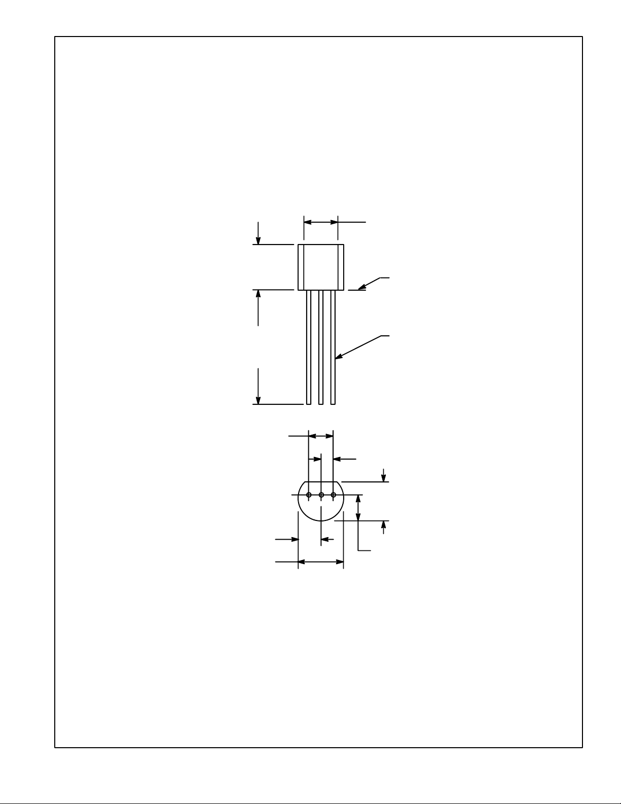
.210
(5.33)
Max
.135 (3.45) Min
Seating Plane
.500
(12.7)
Min
.100 (2.54)
.105 (2.67) Max
.205 (5.2) Max
.021 (.445) Dia Max
B E B2
.050 (1.27)
.165
(4.2)
Max
.105 (2.67) Max
 Loading...